Key Findings
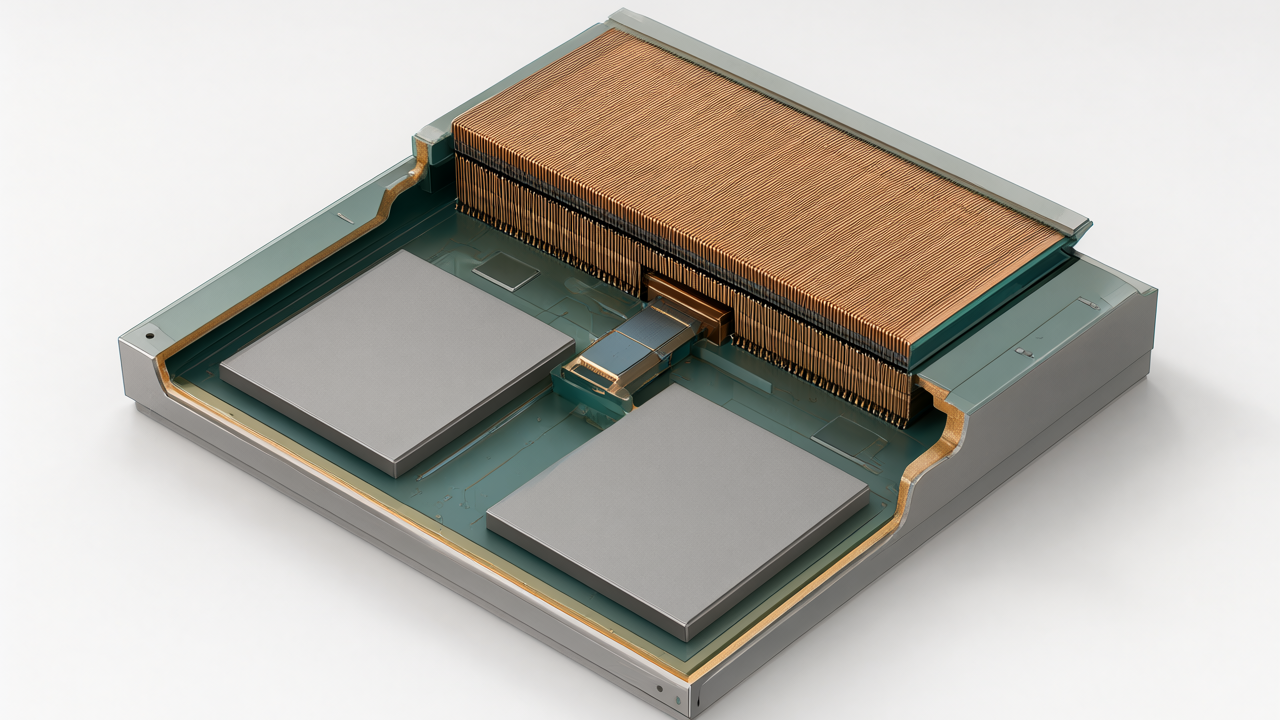
Intel’s Embedded Multi-die Interconnect Bridge (EMIB) is a 2.5D packaging technology that efficiently connects adjacent dies through small silicon bridges embedded within the package substrate. This innovative approach assigns extensive routing and power distribution to the standard package substrate, while reserving ultra-fine pitch routing for critical areas demanding high-bandwidth connectivity. This method eliminates the need for large, expensive silicon interposers across the entire package, thus enabling cost-effective, high-performance multi-die integration.
Technical / Clinical Details
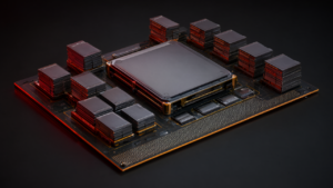
The EMIB architecture is characterized by a compact silicon bridge directly embedded within the dielectric layers of the package substrate. This bridge facilitates ultra-fine pitch wiring between neighboring chiplets, allowing for high-bandwidth, low-latency communication at the chiplet level. Unlike traditional 2.5D packaging solutions that require multiple dies to be placed on a large silicon interposer, EMIB confines this interposer functionality to a localized bridge, significantly reducing manufacturing costs and complexity. For areas outside the bridge, the system relies on a more cost-effective organic package substrate for signal routing and power delivery. This ‘localized interposer’ strategy offers superior flexibility and scalability by providing high-density connectivity only where necessary, while utilizing standard packaging technologies elsewhere. EMIB is particularly well-suited for chiplet processors, AI accelerators, High-Performance Computing (HPC) devices, FPGAs, and packages combining logic chips with High Bandwidth Memory (HBM), enabling these complex systems to seamlessly collaborate within a single package for superior performance.
Background & Context
As the physical limits of Moore’s Law become increasingly apparent, the semiconductor industry has shifted its focus from solely increasing transistor density within a single chip to achieving performance gains through advanced packaging technologies. Chiplet architectures and 2.5D/3D packaging, which integrate multiple functional dies into a single package, have become essential for balancing system performance, power efficiency, and manufacturing costs. Intel’s EMIB emerged within this industry trend as a solution that combines high bandwidth with cost efficiency. While competing technologies like TSMC’s CoWoS (Chip-on-Wafer-on-Substrate) utilize larger silicon interposers, EMIB’s more targeted approach gives it a distinct competitive advantage in specific applications. The tight integration of memory and logic in AI accelerators and HPC is critical for maximizing data processing capabilities, and EMIB provides an effective means to achieve this.
Strategic Significance & Outlook
EMIB technology is expected to play a crucial role in shaping the future of high-performance computing. Particularly with the evolution of AI and the increasing demands for data processing, where closer integration of HBM and logic dies is imperative, technologies like EMIB are key to overcoming bandwidth and power efficiency bottlenecks. In the future, it is anticipated to expand the possibilities for heterogeneous integration, allowing for the combination of more diverse types of chiplets (e.g., analog, RF, security modules) into a single package. This will accelerate the design of custom solutions optimized for specific applications. Intel’s continued evolution of EMIB and its promotion of the chiplet ecosystem are expected to drive innovation across the broader semiconductor industry.
Source: https://www.bestpcbs.com/blog/2026/10/emib/
Get our weekly technology intelligence — free
Receive an infographic that lets you judge at a glance whether each field’s analysis report is worth reading.
Subscribe Free — Weekly Tech Intelligence
By subscribing, you’ll receive Troy-Technical’s weekly technology intelligence newsletter.
- Your email and selected fields are used only to deliver the newsletter.
- We never share your information with third parties.
- You can unsubscribe anytime via the link in each email.
See our Privacy Policy for details.
Takes about a minute · Unsubscribe anytime