


Key Findings
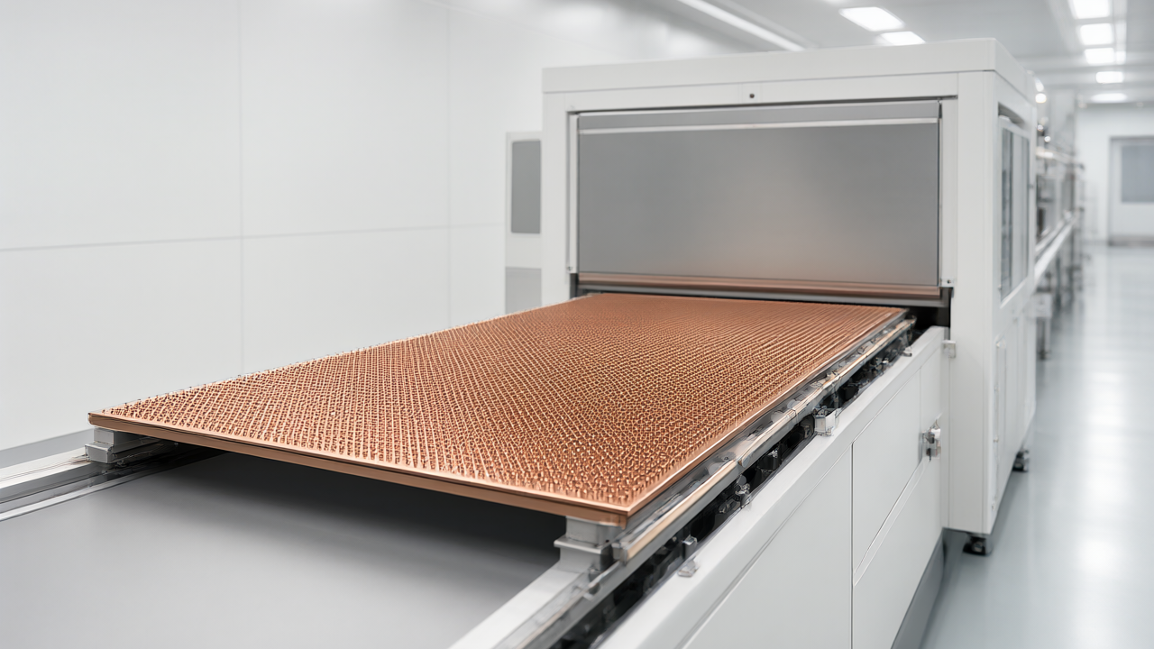
ACM Research has delivered its first 310 × 310 mm Ultra ECP ap-p panel-level horizontal electroplating production system to a customer based in Asia (excluding mainland China). This deployment follows the previous shipment of a 515 × 510 mm R&D tool, signaling the company’s ability to commercialize technical breakthroughs for mass production. The tool is designed to address the industry shift toward larger substrates in advanced packaging.
Technical Details
The Ultra ECP ap-p system utilizes proprietary horizontal electroplating technology and is compatible with copper (Cu), nickel (Ni), tin-silver (SnAg), and gold (Au) plating processes. Key technical specifications include:
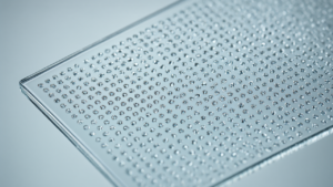
- Copper Plating: Features a high-speed plating paddle optimized for tall copper pillar applications, achieving within-die uniformity for 300-micron copper pillars at high plating rates.
- Deposition Uniformity: Employs patent-pending technology that synchronizes chuck rotation with a rotating rectangular electric field.
- Hardware Reliability: Incorporates a four-sided sealing dry contact chuck.
- Contamination Control: Includes in-cell rinse functionality to minimize chemical cross-contamination between different plating cells.
Background & Context
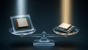
Electroplating is a critical stage in advanced packaging where plating thickness uniformity, consistency, and equipment stability directly impact product yield and manufacturing efficiency. As AI drives the need for increasingly complex packaging architectures, the industry is adopting panel-level processing to accommodate larger substrates compared to traditional wafer-level processing.
Significance & Outlook
According to CEO Dr. David Wang, the shipment of the 310 × 310 mm tool is a milestone in ACM’s advanced packaging efforts. The company positions its horizontal plating technology as a key enabler for next-generation semiconductor packaging across various panel sizes. ACM intends to expand its multi-product platform and global customer base to support the growth of the AI industry.
Get our weekly technology intelligence — free
Receive an infographic that lets you judge at a glance whether each field’s analysis report is worth reading.
Subscribe Free — Weekly Tech Intelligence
By subscribing, you’ll receive Troy-Technical’s weekly technology intelligence newsletter.
- Your email and selected fields are used only to deliver the newsletter.
- We never share your information with third parties.
- You can unsubscribe anytime via the link in each email.
See our Privacy Policy for details.
Takes about a minute · Unsubscribe anytime