
Key Findings
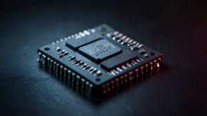
Fraunhofer IPMS is introducing advancements in chiplet integration, silicon nitride (SiN) photonics, and hafnium oxide-based ferroelectric memory. These technologies focus on improving system performance and reducing power consumption through heterogeneous integration and energy-efficient data storage.
Technical Details
The institute’s integration research focuses on two primary methods:
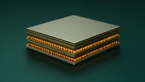
- 2.5D Integration: Utilizing high-density interposers to connect separate logic, memory, and sensor chiplets into compact systems.
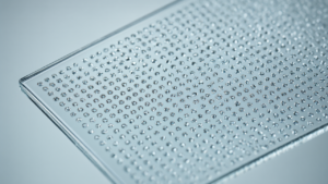
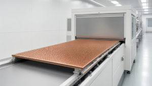
- Quasi-Monolithic Integration (QMI): Embedding chiplets into specially structured pockets within silicon wafers to enable wafer-level interconnections while maintaining modular flexibility.
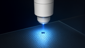
In photonics, Fraunhofer IPMS has developed a silicon nitride (SiN) platform compatible with 200 mm and 300 mm wafers. This platform exhibits extremely low optical losses across wavelengths from visible light to mid-infrared, targeting applications in optical computing, quantum technologies, and photonic biosensors.
Regarding memory, the institute is developing hafnium oxide-based ferroelectric memory, including FeFET and non-volatile FRAM devices. These components operate at voltages below 1 V with nanosecond switching times, designed for edge AI, intelligent sensors, and embedded systems.
Background & Context
These developments are tied to the European APECS pilot line, a component of the EU Chips Act’s Chips for Europe Initiative. Led by Research Fab Microelectronics Germany (FMD) and European partners, APECS provides industry access to advanced packaging and heterogeneous integration. Additionally, the institute utilizes the FAMES European pilot line to facilitate the transfer of these technologies into industrial applications.
Significance & Outlook
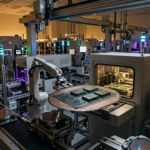
By integrating back-end process technologies into front-end fabrication, Fraunhofer IPMS aims to bridge the gap between laboratory research and commercial manufacturing. The availability of design kits, fabrication services, and technology platforms allows external partners to implement these CMOS-compatible processes into high-volume semiconductor production, enabling the creation of more powerful and energy-efficient systems.
Source: https://www.eenewseurope.com/en/fraunhofer-ipms-advances-chiplet-integration-and-low-power-memory/
Get our weekly technology intelligence — free
Receive an infographic that lets you judge at a glance whether each field’s analysis report is worth reading.
Subscribe Free — Weekly Tech Intelligence
By subscribing, you’ll receive Troy-Technical’s weekly technology intelligence newsletter.
- Your email and selected fields are used only to deliver the newsletter.
- We never share your information with third parties.
- You can unsubscribe anytime via the link in each email.
See our Privacy Policy for details.
Takes about a minute · Unsubscribe anytime