
Key Findings: Hybrid Bonding Evolves into a Scalable Manufacturing Platform for 3D Chip Stacking
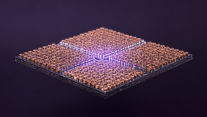
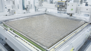
Hybrid bonding is a transformative semiconductor integration technology that directly connects two dies or wafers with copper, bypassing reliance on traditional solder microbumps. This advancement holds the potential to convert 3D chip stacking into a scalable mass manufacturing platform. Notably, in 2026, Imec and EV Group successfully demonstrated wafer-to-wafer (W2W) bonding at a remarkably fine 200nm copper interconnect pitch, proving the high scalability of this technology.
Technical Details: Copper-to-Copper Bonding and Miniaturization Progress
At its core, hybrid bonding involves directly joining exposed copper interconnects on the surfaces of dies or wafers. This direct copper-to-copper bond achieves extremely low electrical resistance and superior thermal conductivity, enabling significantly higher interconnect densities than conventional microbumps. The successful 200nm pitch W2W bonding by Imec and EV Group indicates that this technology has reached the miniaturization levels required for next-generation semiconductors. This allows for the integration of more signal and power lines within a confined space, contributing to enhanced data transfer speeds and reduced power consumption.
Industry Trends and Applications: TSMC’s SoIC and 3nm Chip Stacking
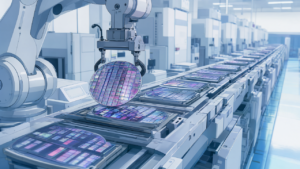
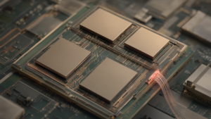
Hybrid bonding is already being implemented by major industry players. TSMC has reported utilizing hybrid bonding, with bond pitches starting below 10 micrometers, in its 3D stacking technology, SoIC (System-on-Integrated Chips). The company’s 3nm chip stacking technology entered mass production in 2025, underscoring the maturity and importance of hybrid bonding at advanced process nodes. This technology is particularly valuable for complex heterogeneous integration applications, such as the highly efficient integration of HBM (High Bandwidth Memory) and logic chips essential for AI processors.
Future Outlook: Pushing the Boundaries of Semiconductor Performance
As discussions around the limits of Moore’s Law intensify, hybrid bonding technology stands as one of the primary drivers for further semiconductor performance improvement. Coupled with advancements in chiplet design and 3D stacking technologies, this bonding method enables the creation of higher-performance, lower-power, and more compact next-generation electronic devices. Continuous investment and innovation by research institutions and leading manufacturers are expected to lead to even finer miniaturization and broader adoption of hybrid bonding in the coming years. This will accelerate technological breakthroughs in fields such as AI, 5G/6G communication, autonomous vehicles, and high-performance data centers.
Get our weekly technology intelligence — free
Receive an infographic that lets you judge at a glance whether each field’s analysis report is worth reading.
Subscribe Free — Weekly Tech Intelligence
By subscribing, you’ll receive Troy-Technical’s weekly technology intelligence newsletter.
- Your email and selected fields are used only to deliver the newsletter.
- We never share your information with third parties.
- You can unsubscribe anytime via the link in each email.
See our Privacy Policy for details.
Takes about a minute · Unsubscribe anytime





Comments