Key Findings
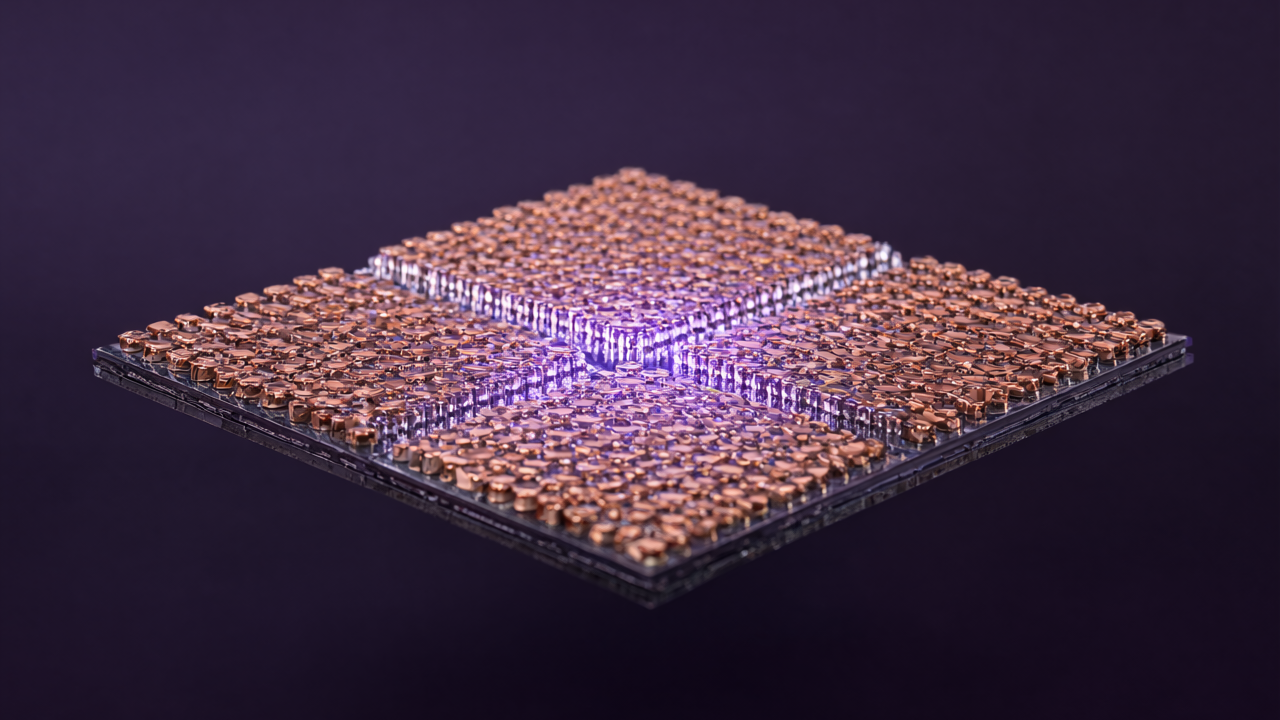
Huawei’s Kirin 9050 Pro chip has been released, featuring cutting-edge hybrid bonding technology with an ultra-fine pitch of 1.5 micrometers. This advancement is central to Huawei’s ‘logic folding’ technique, which promises to enhance chip operating frequencies without solely relying on traditional miniaturization. A roadmap indicates projected performance increases from 3.1GHz in 2026 to 4.3GHz by 2030.
Technical & Clinical Details
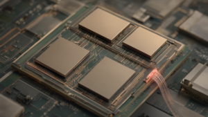
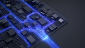
Huawei’s logic folding technology involves directly bonding two chips face-to-face, connecting them with an extremely short pitch. As this bonding pitch approaches the physical wiring density, the two physically separate chips electrically behave as a single, integrated unit, enabling seamless data transfer and signal integrity. Unlike conventional packaging methods that rely on pins or bumps, introducing inherent distance and resistance, hybrid bonding facilitates direct copper-to-copper connections, significantly mitigating these limitations. The 1.5μm pitch adopted in the Kirin 9050 Pro is among the finest in commercial hybrid bonding technologies, maximizing inter-chiplet bandwidth and minimizing latency. This technique effectively boosts clock frequencies and overall system performance without necessarily requiring further physical circuit miniaturization.
Background & Context
The semiconductor industry is grappling with the fundamental limits of Moore’s Law, making innovation in packaging technology indispensable for continued performance gains. Hybrid bonding is gaining prominence as a key enabler for chiplet technology and 3D stacking. Huawei’s achievement underscores its continued commitment to high-performance chip development through unique technological innovation, even under US sanctions, highlighting China’s growing presence in the global semiconductor technology race.
Strategic Significance & Outlook
Huawei’s roadmap for hybrid bonding and logic folding technology signals the future direction of advanced packaging in the semiconductor industry. The goal of increasing operating frequencies to 4.3GHz by 2030 holds significant implications for various high-speed processing applications, including AI, high-performance computing, and mobile communications. Further advancements and widespread adoption of this technology will enhance chip design flexibility, accelerating the development of more powerful and energy-efficient next-generation semiconductors. The performance enhancements delivered by hybrid bonding are expected to be a critical factor in future technological innovation.
Source: https://www.investlingo.jp/content/3JWkjyTxMqk4CB41014R9dvZ3Rg
Get our weekly technology intelligence — free
Receive an infographic that lets you judge at a glance whether each field’s analysis report is worth reading.
Subscribe Free — Weekly Tech Intelligence
By subscribing, you’ll receive Troy-Technical’s weekly technology intelligence newsletter.
- Your email and selected fields are used only to deliver the newsletter.
- We never share your information with third parties.
- You can unsubscribe anytime via the link in each email.
See our Privacy Policy for details.
Takes about a minute · Unsubscribe anytime




Comments