Key Findings
At SEMICON West 2026, the SEMI Startups for Sustainable Semiconductors program highlighted four innovative companies presenting solutions to critical industry challenges. Key advancements include HEXAspec Inc.’s high-thermal-conductivity encapsulation, CHIPADD, Corp.’s direct-printed copper cooling, K1 Semiconductor’s novel wafer splitting, and FS2’s monolithic 3D integration for SRAM.
Technical Details
- HEXAspec Inc. – Advanced Encapsulation Molding Materials: HEXAspec has developed a new encapsulation molding material leveraging hexagonal boron nitride (hBN) nanosheets within a polymer matrix. This material achieves a thermal conductivity 10 times higher than conventional options while preserving essential electrical insulation and mechanical strength. This innovation is crucial for managing the increasing heat density in advanced semiconductor packages.
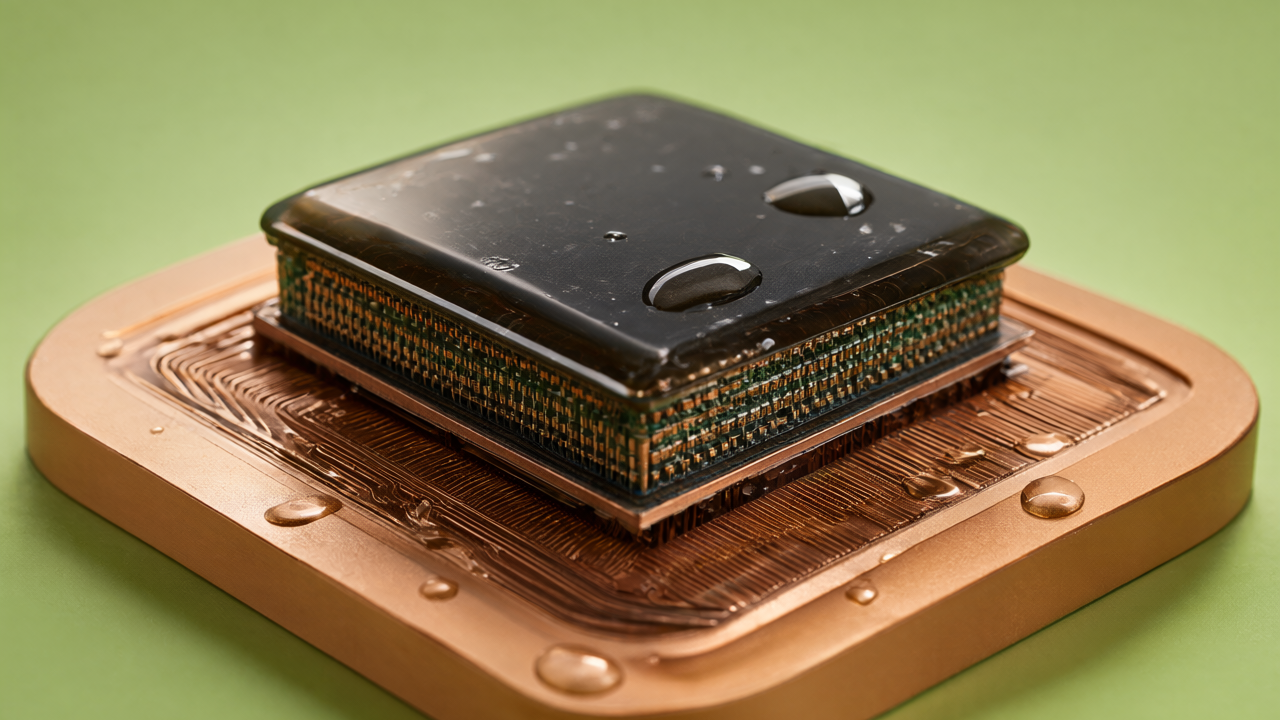
- CHIPADD, Corp. – Ultra-Efficient Copper Cooling: CHIPADD introduced a technology for directly additive manufacturing ultra-efficient copper cooling features onto the surfaces of high-power chips like GPUs and CPUs. This process includes robust bonding materials to ensure durable adhesion and efficient heat transfer, significantly enhancing thermal dissipation at the chip level and pushing performance boundaries for AI and high-performance computing (HPC) applications.
- K1 Semiconductor – Patented Wafer Splitting Method: K1 Semiconductor presented a patented method for cleaving thin layers from high-quality single-crystal parent wafers. This technique enables the production of thinner, more flexible custom semiconductor wafers, offering new design possibilities for 3D stacking and heterogeneous integration, which are vital for compact and powerful devices.
- FS2 – Monolithic 3D Integration Platform: FS2 showcased a monolithic 3D integration platform and memory designed for building next-generation stacked 3D SRAM and process-on-memory architectures. This platform aims to minimize the physical distance between memory and logic, thereby reducing data transfer latency and power consumption, addressing key bottlenecks in advanced computing systems.
Background & Context
The semiconductor industry faces dual pressures: the physical limits of Moore’s Law scaling and the growing imperative for sustainable manufacturing practices. Innovations in materials science, thermal management, and advanced packaging are therefore paramount. The SEMI Startups for Sustainable Semiconductors program serves as a critical platform to foster and promote companies offering groundbreaking solutions in these areas. The presented technologies reflect a holistic approach to improving semiconductor performance, efficiency, and environmental footprint.
Strategic Significance & Outlook
The technologies introduced by these startups are poised to play a significant role in shaping the future of semiconductor manufacturing. HEXAspec and CHIPADD’s thermal management solutions will be instrumental in unlocking higher performance in AI and HPC processors by mitigating thermal throttling and reducing power consumption. K1 Semiconductor’s wafer technology could accelerate the development of more compact and higher-performing 3D stacked devices. FS2’s monolithic 3D integration offers a pathway to fundamentally alter computing architectures by resolving data bottlenecks. Collectively, these innovations promise to enhance the competitiveness of the semiconductor industry and drive a more sustainable technological evolution across various high-growth sectors.
Get our weekly technology intelligence — free
Receive an infographic that lets you judge at a glance whether each field’s analysis report is worth reading.
Subscribe Free — Weekly Tech Intelligence
By subscribing, you’ll receive Troy-Technical’s weekly technology intelligence newsletter.
- Your email and selected fields are used only to deliver the newsletter.
- We never share your information with third parties.
- You can unsubscribe anytime via the link in each email.
See our Privacy Policy for details.
Takes about a minute · Unsubscribe anytime







Comments