Key Findings
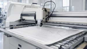
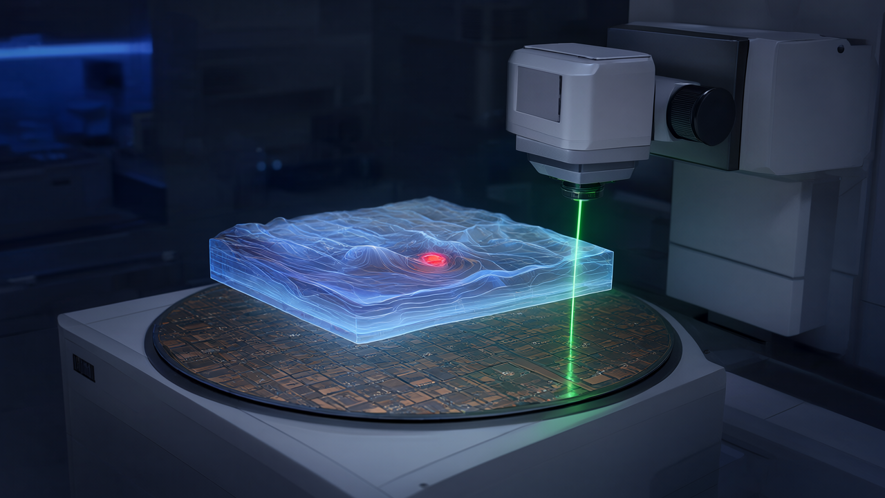
In advanced packaging technology, 3D metrology is significantly improving defect detection capabilities, proactively preventing costly failures in hybrid bonding and complex chiplet integrations. This technology enables high-precision measurement of minute bump heights and surface profiles, facilitating early identification of small defects that might otherwise go unnoticed by conventional inspection methods.
Technical & Clinical Details
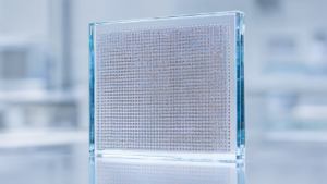
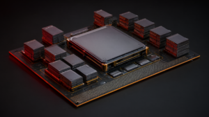
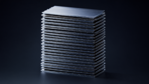
The assembly of chiplets, high-bandwidth memory (HBM) stacks, and hybrid-bonded devices in advanced semiconductor packaging involves substantial material and process resources. Undetected defects at early stages of this intricate manufacturing flow can jeopardize the entire larger assembly, leading to significant financial losses. For instance, micron-level variations in fine bump heights or nanometer-scale surface roughness on bonding interfaces can cause performance degradation and reliability issues. 3D metrology non-destructively and rapidly scans these microstructures, acquiring three-dimensional shape data. This allows for precise localization, sizing, and characterization of defects. This capability enables manufacturers to more thoroughly characterize increasingly complex structures and enhance process control.
Background & Context
As Moore’s Law approaches its physical limits, the semiconductor industry is shifting towards advanced packaging technologies to drive performance improvements and cost reductions. However, techniques like multi-layer chiplet stacking and hybrid bonding dramatically increase manufacturing complexity and, concurrently, the difficulty of defect detection. The impact is particularly severe when defects are discovered after expensive materials and lengthy processes have been invested. Therefore, the ability to accurately detect defects early in the assembly process is a critical factor for ensuring the yield and reliability of advanced packaging.
Strategic Significance & Outlook
The evolution of 3D metrology is key to overcoming challenges faced by semiconductor manufacturers, enabling the mass production of next-generation high-performance chips. Future advancements are expected in faster and more precise 3D metrology equipment, alongside integration with AI-powered data analytics for real-time process control. This will further boost manufacturing yields and improve overall semiconductor quality and cost efficiency. Ultimately, this will accelerate the development of fields reliant on advanced semiconductors, such as AI and High-Performance Computing (HPC).
Get our weekly technology intelligence — free
Receive an infographic that lets you judge at a glance whether each field’s analysis report is worth reading.
Subscribe Free — Weekly Tech Intelligence
By subscribing, you’ll receive Troy-Technical’s weekly technology intelligence newsletter.
- Your email and selected fields are used only to deliver the newsletter.
- We never share your information with third parties.
- You can unsubscribe anytime via the link in each email.
See our Privacy Policy for details.
Takes about a minute · Unsubscribe anytime