

Key Findings
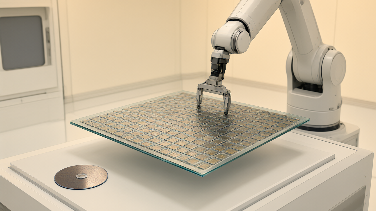
Moving from wafer-level to panel-level packaging dramatically improves area utilization, particularly for large rectangular AI and HPC packages. For a 5.5×-reticle-size interposer, a 300mm wafer produces 9 units, whereas a 600mm panel produces 72 units—an eightfold increase in utilization. Intel Foundry demonstrated a similar advantage with a 4× reticle package, producing approximately 48 units on a 510 × 515mm panel compared to 10 units on a 300mm wafer.
Technical Details
The transition introduces significant mechanical and process challenges:
- Geometry and Coating: Traditional spin coating relies on radial symmetry, which causes uneven film thickness on rectangular panels. Consequently, 600mm panel flows utilize slit or slot-die coating across active areas of roughly 586 × 586mm.
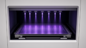
- Lithography: Conventional wafer steppers are being displaced by maskless direct imaging in many panel flows.
- Process Control: While wafer processing is typically single-sided, panel processing is dual-sided, complicating uniformity and Cpk (process capability index).
- Precision: As line and space dimensions move from 5µm toward 2µm and below, panel processes require precision closer to front-end manufacturing.
Background & Context
The industry has spent decades optimizing equipment and materials for round 300mm wafers. Because the largest square that fits on a 300mm wafer is only about 210 × 210mm, panels have become an obvious choice for the scaling needs of AI systems. However, the manufacturing infrastructure is not yet fully ready for the larger format.
Significance & Outlook
Due to high risks in assembly on 600mm panels, some manufacturers are adopting a compromise: completing the interposer in a large 600mm format and then dividing it into four 300mm pieces for assembly and the C4 process. This approach yields 64 units—fewer than a full intact panel but significantly more than a wafer. This transition reveals that many “process requirements” were actually dependencies on wafer geometry, necessitating a new manufacturing process rather than a simple scale-up.
Source: https://semiengineering.com/what-breaks-when-packaging-moves-from-wafer-to-panel/
Get our weekly technology intelligence — free
Receive an infographic that lets you judge at a glance whether each field’s analysis report is worth reading.
Subscribe Free — Weekly Tech Intelligence
By subscribing, you’ll receive Troy-Technical’s weekly technology intelligence newsletter.
- Your email and selected fields are used only to deliver the newsletter.
- We never share your information with third parties.
- You can unsubscribe anytime via the link in each email.
See our Privacy Policy for details.
Takes about a minute · Unsubscribe anytime