

Key Findings
Lam and imec have entered a collaboration to accelerate manufacturing readiness for 3D integration technologies. By combining Lam’s deposition and etch capabilities with imec’s integration infrastructure, the partnership aims to scale heterogeneous integration and advanced packaging across the industry. Additionally, the two organizations are collaborating on the application of Lam’s Aether dry resist platform to address the requirements of high-NA EUV lithography.
Technical Details
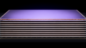
Joint research in 3D integration covers several critical process areas:
- Thick dielectric deposition, asymmetric stress compensation, bevel deposition, and plasma dicing.
- Process validation for advanced packaging and future memory architectures.
- Future 3D memory technologies, including new charge-trap materials, precision multilayer deposition, high-aspect-ratio channel etch, deep memory contacts, and low-resistivity interconnects.
Regarding logic devices, the collaboration focuses on enhancing the resolution, sensitivity, depth of focus, and stochastic defectivity of the Aether dry resist platform using imec’s high-NA EUV environment. This includes exploring ruthenium direct metal etch for advanced interconnects at aggressive pitches. Joint research has already demonstrated single-exposure high-NA EUV patterning for sub-20 nm ruthenium direct metal etch interconnects, achieving 100% electrical yield for fork structures and over 90% for meander structures at a 20nm pitch.
Background & Context
The push toward 3D integration and high-NA EUV is driven by AI workloads that require increased memory density and bandwidth. As the industry moves toward angstrom-era nodes, high-NA EUV is necessary for smaller features and higher transistor density, though it requires simultaneous innovations in resists, mask design, patterning, and materials.
Significance & Outlook
The Aether platform, alongside Lam’s Akara etch systems and Striker ALD portfolio, provides a path toward reducing multi-patterning complexity and improving manufacturability. These innovations are intended to enable the gate-all-around (GAA) and complementary FET (CFET) architectures expected to power future generations of AI computing.
Source: https://www.electronicsweekly.com/news/business/lam-and-imec-pursue-3-d-integration-2026-10/
Get our weekly technology intelligence — free
Receive an infographic that lets you judge at a glance whether each field’s analysis report is worth reading.
Subscribe Free — Weekly Tech Intelligence
By subscribing, you’ll receive Troy-Technical’s weekly technology intelligence newsletter.
- Your email and selected fields are used only to deliver the newsletter.
- We never share your information with third parties.
- You can unsubscribe anytime via the link in each email.
See our Privacy Policy for details.
Takes about a minute · Unsubscribe anytime