


Key Findings
A joint research team has successfully reduced the contact resistance of WSe2 transistors from 1,869 ohm-micrometers to 104 ohm-micrometers, representing a reduction of approximately 94%. Additionally, the hole mobility of the material increased from 55 cm²V⁻¹s⁻¹ to 218.3 cm²V⁻¹s⁻¹. These improvements were achieved through a novel oxygen doping process that repairs selenium vacancies and optimizes the metal-semiconductor interface.
Technical Details
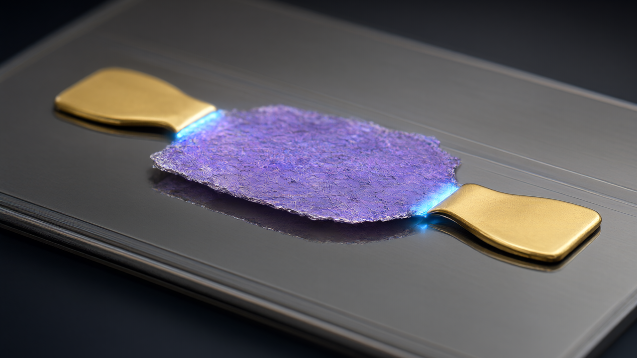
The team utilized oxygen atoms to fill selenium vacancies within the WSe2 structure, forming stable chemical bonds that smooth the electronic structure of the interface. The researchers compared two process sequences and found that “post-doping”—applying oxygen annealing after the fabrication of metal electrodes—was significantly more effective. This method allows oxygen to penetrate through microscopic gaps in the metal, creating a near-perfect Ohmic contact while avoiding damage to the material that can occur during pre-doping.
To further optimize performance, the team implemented a “full-contact” structure combining top and edge contacts to maximize the contact area and minimize energy loss. In a device with a channel length of 16 nm, the transistor achieved a saturation current of 1,635 microamps per micrometer and a ballistic transport ratio of 81% at room temperature.
Background & Context
As silicon reaches its physical limits regarding leakage and heat generation, 2D semiconductor materials—which are only one atom thick—have emerged as candidates for next-generation chips. While n-type transistors have progressed, p-type transistors using WSe2 have been hindered by high contact resistance and selenium vacancies, which act as obstacles to hole movement.
Significance & Outlook
The results demonstrate that 2D p-type transistors can outperform previous silicon-based devices in specific metrics, clearing a major hurdle for sub-1 nm chip development. However, the researchers note that transitioning from silica substrates to high-k dielectric insulating layers and achieving large-scale, uniform material growth in factory environments remain the primary challenges for commercialization.
Source: https://news.qq.com/rain/a/20261112A096Z000
Get our weekly technology intelligence — free
Receive an infographic that lets you judge at a glance whether each field’s analysis report is worth reading.
Subscribe Free — Weekly Tech Intelligence
By subscribing, you’ll receive Troy-Technical’s weekly technology intelligence newsletter.
- Your email and selected fields are used only to deliver the newsletter.
- We never share your information with third parties.
- You can unsubscribe anytime via the link in each email.
See our Privacy Policy for details.
Takes about a minute · Unsubscribe anytime