

Key Findings
imec has established a technical reference platform for silicon interposer technology as part of the NanoIC pilot line. This platform provides the baseline flows necessary to develop a dedicated silicon interposer Process Design Kit (PDK), which is scheduled for release in early 2027. The PDK will allow universities, start-ups, and fabless companies to utilize industry-standard EDA environments from Cadence and Synopsys to virtually explore advanced packaging before moving to physical manufacturing.
Technical Details
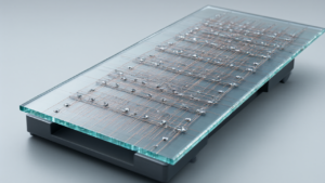
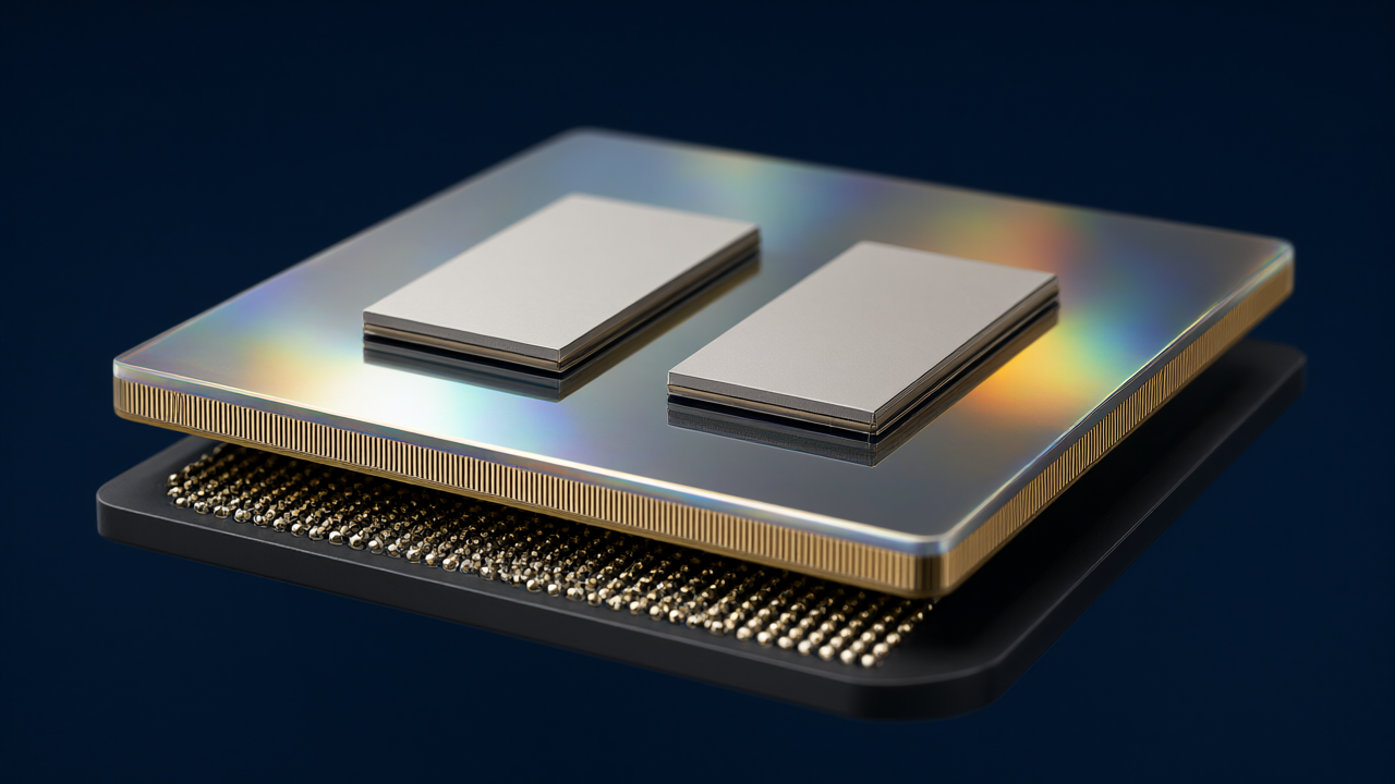
The silicon interposer platform serves as a high-density routing layer positioned beneath dies to link compute chiplets, high-bandwidth memory, and specialized components. Key technical specifications include:
- Support for microbump pitches down to 20 µm.
- Integration of through-silicon vias (TSVs).
- Multiple metal routing layers for 2.5D packaging.
This technology is one of three interconnect solutions being developed within NanoIC, alongside fine-pitch RDL interposers and die-to-wafer hybrid bonding. While silicon interposers focus on high-density routing for advanced compute, fine-pitch RDL interposers provide a cost-efficient alternative, and hybrid bonding enables ultra-dense chip-to-chip connections.
Background and Context
The development addresses the rising performance requirements of AI accelerators and GPUs, where bandwidth and energy-efficient data movement are critical. The NanoIC pilot line is jointly funded by the Chips Joint Undertaking via the European Union’s Digital Europe and Horizon Europe programs, with participation from Belgium (Flanders), France, Germany, Finland, Ireland, and Romania.
Significance and Outlook
By providing a common technology foundation and accessible PDKs, imec aims to allow designers to experiment with different interconnect approaches and evaluate system architectures. The long-term goal of NanoIC is to transition from virtual exploration via PDKs to the creation of physical silicon demonstrators on the pilot line. This infrastructure is intended to help European markets prepare for next-generation automotive, physical AI, and advanced computing systems.
Get our weekly technology intelligence — free
Receive an infographic that lets you judge at a glance whether each field’s analysis report is worth reading.
Subscribe Free — Weekly Tech Intelligence
By subscribing, you’ll receive Troy-Technical’s weekly technology intelligence newsletter.
- Your email and selected fields are used only to deliver the newsletter.
- We never share your information with third parties.
- You can unsubscribe anytime via the link in each email.
See our Privacy Policy for details.
Takes about a minute · Unsubscribe anytime