New Technology– category –
-

HBM Packaging: Samsung vs SK Hynix patent competition in 2026
BigGo Finance South Korea Overview Samsung Electronics and SK Hynix have filed competing patents in the U.S. for advanced HBM packaging, aiming to enhance efficiency and reliability. Samsung proposes integrating pre- and post-bonding ins... -
HBM4E: Samsung’s 4nm base die and thermal specs for NVIDIA
East Asia Brief South Korea Overview Samsung Electronics has developed an advanced HBM4E thermal management solution featuring a 4nm logic-based die and hybrid copper bonding (HCB), slashing thermal resistance by over 20% compared to HBM... -
Brewer Science: High-temp laser debonding specs for IMAPS 2026
Brewer Science USA Overview Brewer Science presented new data at IMAPS 2026 on its high-temperature resistant laser debonding materials specifically designed for advanced packaging Temporary Bonding/Debonding (TBDB) applications. This ne... -
Resonac: First Japanese 12-inch SiC single crystal substrate
Semicon electronics Japan Overview Resonac Holdings announced the successful manufacturing and subsequent substrate processing of a 300mm (12-inch) SiC single crystal on September 15, 2026. This achievement marks a first for a Japanese c... -
ERS electronic: Automated PLP system for 310x310mm substrates
Chiplet Marketplace Germany Overview ERS electronic has introduced a fully automated Panel-Level Packaging (PLP) system designed to enhance AI and chiplet architectures. This innovative system handles 310x310mm substrates, integrating th... -
JDI Mobara Plant: Shinko Electric and FICT 2028 operation plan
EE Times Japan Japan Overview Shinko Electric Industries and FICT have acquired Japan Display's (JDI) Mobara plant in Chiba Prefecture, designating it as a core facility for advanced AI semiconductor packaging, with operations slated to ... -
Cu-to-Cu Hybrid Bonding: Semiconductor backend specs explained
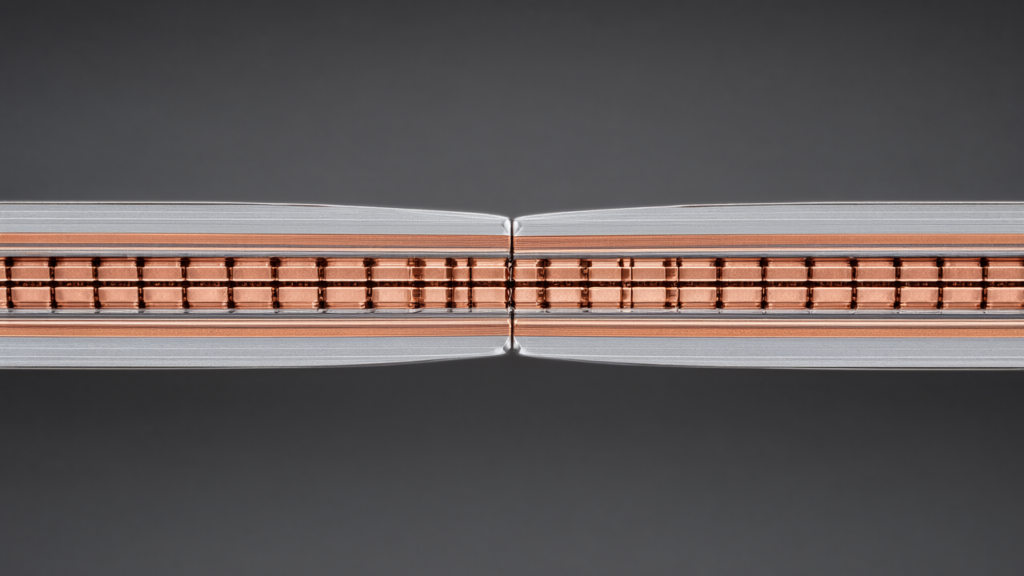
GenInnov USA Overview In semiconductor manufacturing, packaging, particularly pitch miniaturization in "vertical competition," is key to performance and cost reduction. Copper-to-copper hybrid bonding is emerging as a major breakthrough,... -
NVHBM: Micron’s NVIDIA custom base die specs and 15% power cut
The Elec Inc. South Korea Overview Micron will outsource the base die for its custom NVHBM product, developed for NVIDIA and based on HBM4E, anticipating enhanced profitability. NVHBM achieves a 15% reduction in power consumption and up ... -
Samsung zHBM: 3D architecture specs for 8x performance gains
PhotonCap South Korea Overview Samsung has introduced zHBM, an innovative 3D memory architecture concept that directly stacks High Bandwidth Memory (HBM) atop the processor, drastically shortening data paths and integrating dedicated coo... -
Samsung HBM4E: Hybrid Copper Bonding cooling specs explained
CHOSUNBIZ South Korea Overview Samsung Electronics is intensifying efforts to manage the escalating heat generated by HBM4E, driven by dramatically expanding interposer sizes for AI semiconductors. The company is adopting Hybrid Copper B...