Key Findings
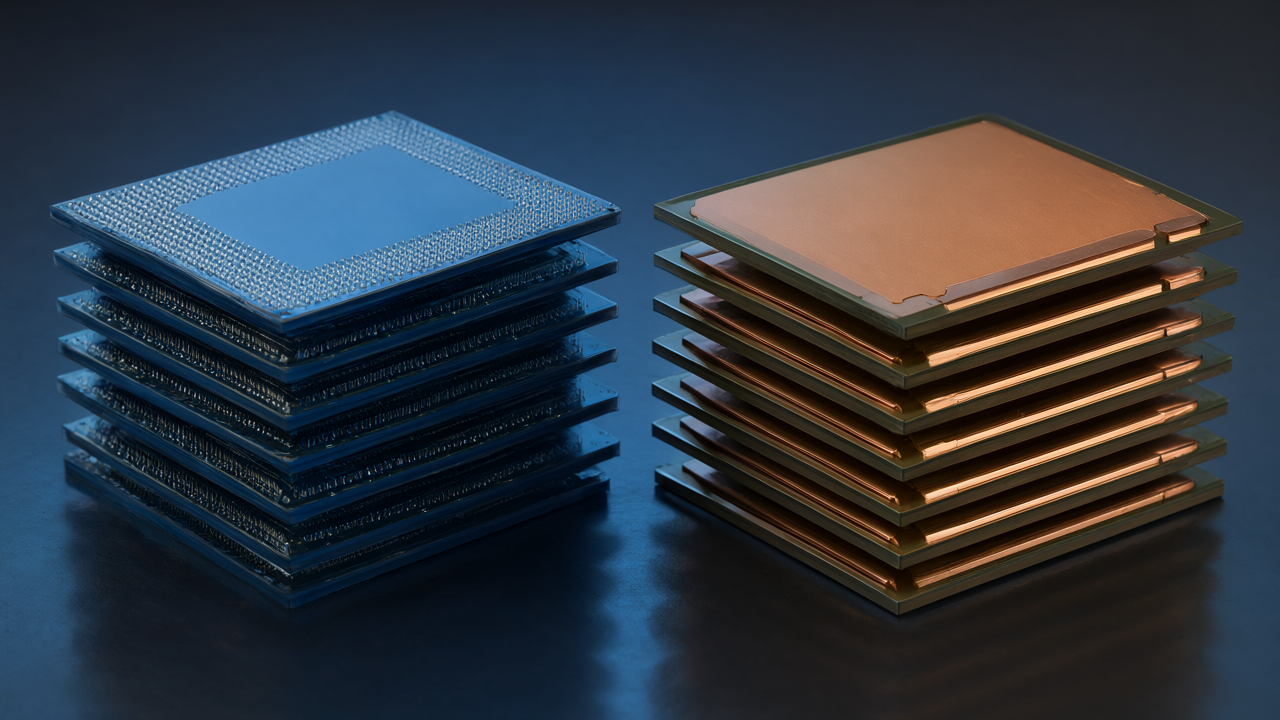
Samsung Electronics and SK Hynix are at the forefront of the advanced packaging race for High Bandwidth Memory (HBM), each filing innovative patents with the U.S. Patent and Trademark Office. Samsung’s proposed technology integrates pre- and post-bonding inspection marks into a single structure, aiming to reduce chip area, significantly enhance alignment precision, and effectively mitigate voids and delamination at the bonding interface. SK Hynix, in parallel, has introduced a design that incorporates polyimide for over 50% of the insulation layer within the HBM stack, effectively suppressing cracks caused by thermal deformation. These patents promise substantial advancements in HBM reliability and manufacturing efficiency.
Technical / Clinical Details
Samsung’s patent focuses on streamlining the manufacturing process for stacked chips. By consolidating traditionally separate pre-bonding and post-bonding inspection marks into a singular structure, the technology minimizes the required footprint for these marks, optimizing valuable chip area. This integration also enables highly precise alignment with a single mark, reducing positional inaccuracies during chip stacking. Consequently, it lowers the risk of defects such as voids and delamination at the bonding interfaces, crucial for improving HBM yield rates and ensuring long-term reliability. SK Hynix’s innovation, conversely, targets thermal management and structural stability within HBM stacks. Multi-layered HBM dies undergo repeated expansion and contraction during operation due to temperature fluctuations, which can induce stress concentrations and lead to cracking. Their proposed design utilizes polyimide, a high-performance polymer known for its excellent heat resistance and flexibility, for more than 50% of the insulation layer. This material choice effectively mitigates internal stresses caused by thermal deformation, preventing crack formation and significantly enhancing the HBM’s durability and reliability for operation in more demanding environments.
Background & Context
The explosive growth of AI and High-Performance Computing (HPC) has made HBM a critical determinant of GPU and AI accelerator performance. As HBM stack counts continue to increase, from HBM3E to HBM4 and beyond, efficient chip area utilization, stacking precision, and robust thermal management have become paramount challenges. The quality of bonding interfaces directly impacts signal integrity and heat dissipation, making defect reduction essential. Furthermore, thermal cycling stress in multi-layered stacks represents a significant concern for package reliability. These patents from Samsung and SK Hynix reflect their strategic efforts to address these challenges and establish technological leadership, thereby accelerating the mass production and adoption of next-generation HBM.
Strategic Significance & Outlook
These advanced packaging patents sought by both companies are expected to contribute not only to HBM manufacturing cost reduction and yield improvement but also to a substantial enhancement in product reliability and durability. This will allow HBM to expand its application scope as a core component of more powerful and stable AI systems. Samsung’s integrated inspection mark technology has the potential to become a standard for fine alignment in future chiplet and 3D stacking technologies, while SK Hynix’s thermal deformation suppression technology will be crucial for ensuring stable HBM operation in extreme conditions. These technological innovations are poised to solidify both companies’ leadership in the AI semiconductor market and positively impact the entire HBM supply chain.
Source: https://finance.biggo.com/news/e9f952bd-5cef-43b9-b4f6-2da0d476dade
Get our weekly technology intelligence — free
Receive an infographic that lets you judge at a glance whether each field’s analysis report is worth reading.
Subscribe Free — Weekly Tech Intelligence
By subscribing, you’ll receive Troy-Technical’s weekly technology intelligence newsletter.
- Your email and selected fields are used only to deliver the newsletter.
- We never share your information with third parties.
- You can unsubscribe anytime via the link in each email.
See our Privacy Policy for details.
Takes about a minute · Unsubscribe anytime