New Technology– category –
-

Hybrid Bonding: Technical Process, Performance and 2026 Roadmap
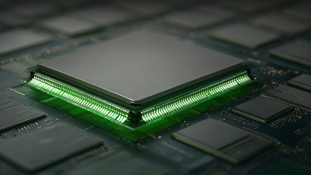
IMAPS 3D InCites Content Platform USA Overview Hybrid bonding enables interconnect pitches below 10um, with Applied Materials and imec/EV group demonstrating pitches of 450nm and 200nm respectively. By eliminating solder bridging and und... -
ASE PowerSiP™: 3D SiP for AI Vertical Power Delivery Specs
ASE Technology Holding USA Overview ASE has expanded its PowerSiP™ platform with a 3D System-in-Package (SiP) solution that enables vertically integrated voltage regulator modules (VRMs). This architecture can reduce parasitic routing lo... -
RF GaN Patents: Chinese Players Lead New Inventions in Q2 2026
Editorial policy: This article was independently reviewed and edited by Troy Technical based on information provided to our editorial team by KnowMade and on the company's publicly available materials. KnowMade analysis Global RF GaN Pat... -
Elephantech: Toyosu Packaging Center 2027 launch and specs
Evertiq Japan Overview Japanese PCB and substrate technology developer Elephantech announced it will open its new Toyosu Advanced Packaging Center in Tokyo by March 2027. This center aims to significantly scale up manufacturing and R&... -
3D Metrology explained: Hybrid bonding defect detection specs
Semiconductor Engineering USA Overview 3D metrology is critically enhancing defect detection in advanced semiconductor packaging, particularly for hybrid bonding, to prevent costly failures. This technology precisely measures fine bump h... -
HBM4: SK hynix and Samsung 16-layer vs NVIDIA 12-layer specs
The Korea Herald South Korea Overview Despite NVIDIA's Vera Rubin AI platform favoring 12-layer HBM4 chips, SK hynix and Samsung Electronics are aggressively pursuing 16-layer HBM4 technology. Samsung leads in hybrid copper bonding for h... -
Ultra C and Ultra ECP: PLP yield and cost efficiency specs
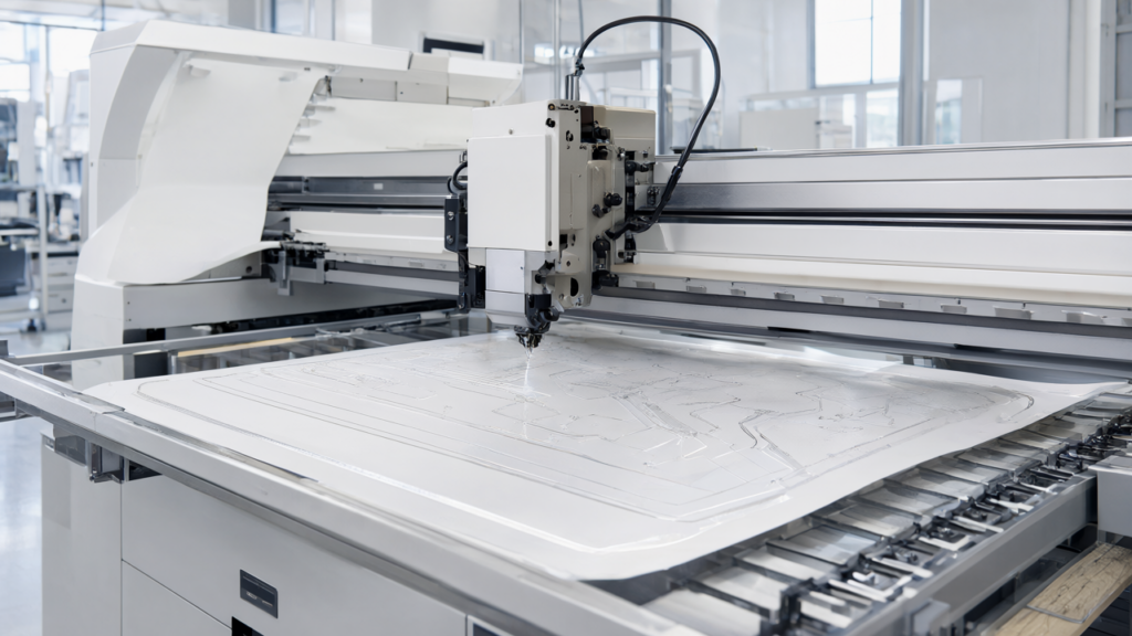
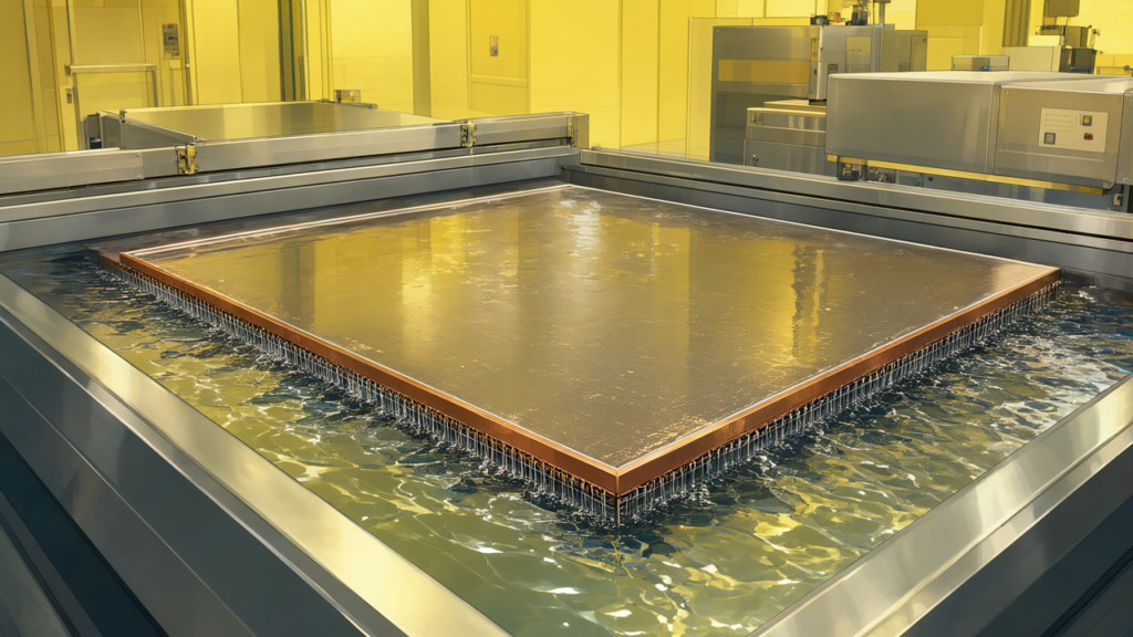
chiplet-marketplace.com Global Overview Ultra C vac-p and Ultra ECP ap-p systems have been developed to overcome critical cleaning and plating challenges in Panel-Level Packaging (PLP). Ultra C vac-p is essential for flux residue removal... -
NVHBM: Micron’s bandwidth and power specs for NVIDIA
The Elec Inc. USA Overview Micron Technology announced its custom HBM product, NVHBM, developed for NVIDIA, will utilize outsourced base dies. NVIDIA states NVHBM integrates a customized physical layer (PHY) to reduce I/O PHY package are... -
Intel EMIB: 2.5D packaging for HBM and logic explained
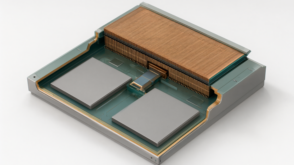
bestpcbs.com USA Overview Intel's EMIB (Embedded Multi-die Interconnect Bridge) is a 2.5D packaging technology that connects adjacent dies via small silicon bridges embedded within the package substrate, achieving high-bandwidth links. W... -
zHBM: Samsung’s vertical stacking and HBM4 performance specs
MK South Korea Overview Samsung Electronics has doubled HBM4's I/O pin count compared to HBM3E, significantly accelerating data transfer with AI accelerators. The company is developing zHBM, a next-generation vertical stacking technology...