

Key Findings
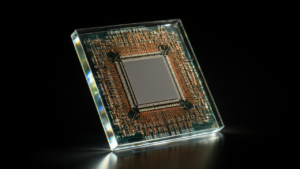
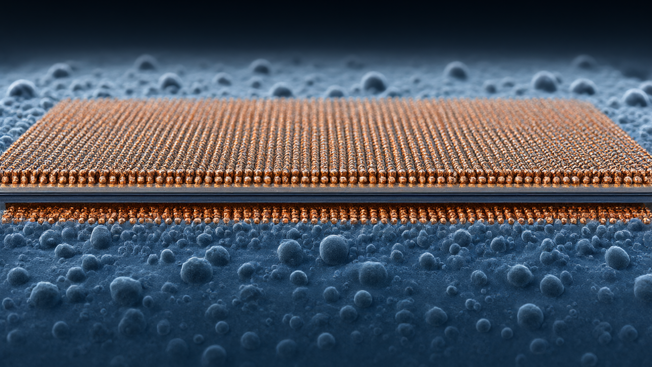
Hybrid bonding significantly increases interconnect density compared to conventional bump limits. At ECTC 2026, Applied Materials demonstrated a 450nm pitch with 98% yield across 20M interconnects, while imec/EV group achieved a 200nm pitch with less than 40nm overlay for 300mm Wafer to Wafer (W2W) bonding. These advancements allow for interconnect pitches as low as 1um, far surpassing the 20um limit of Cu Pillars or the 50um limit of C4 bumps.
Technical Details
The process involves both direct Cu-Cu and dielectric bonding, using either organic polymers or inorganic dielectrics (Si x O y, Si x O y N z, Si x C y N z). There are three primary implementation methods:
- Die to Die (D2D): Bonds two individual dies; limited throughput.
- Die to Wafer (D2W): Places known-good die on a wafer via room temperature oxide bonds; offers flexibility but increases processing time.
- Wafer to Wafer (W2W): Bonds two wafers simultaneously; cost-efficient for simple 2-hi stacks like compute-DRAM or CMOS imagers, though it compounds yield loss.
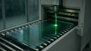
A critical technical requirement is CMP uniformity. While a controlled Cu recess is necessary to prevent oxide separation during expansion, over-dishing or under-dishing of the copper can lead to bond failures.
Background and Context
Cu-Cu Hybrid bonding was invented between 2004-2005, combining embedded metal bonds with ZiBond (direct oxide-to-oxide bond). Sony has used the technology in high-volume production for CMOS image sensors since 2015. The IP landscape has seen significant shifts, including Tessera Technologies’ acquisition of Ziptronix and DTS. Recently, Adeia Inc. settled a patent infringement suit against AMD’s 3D V-Cache processors in March 2026 via a multi-year license agreement.
Significance and Outlook
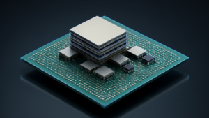
Hybrid bonding reduces vertical interconnect height and thermal interface resistance by eliminating the underfill gap. While more expensive than Thermocompression bonding (TCB) due to stringent processing requirements, it is essential for high-performance interfaces, including high-density chiplet bridges and 224Gbps+ EIC/PIC-based optical engines.
Source: https://www.3dincites.com/2026/10/why-hybrid-bonding-is-hard-to-perfect/
Get our weekly technology intelligence — free
Receive an infographic that lets you judge at a glance whether each field’s analysis report is worth reading.
Subscribe Free — Weekly Tech Intelligence
By subscribing, you’ll receive Troy-Technical’s weekly technology intelligence newsletter.
- Your email and selected fields are used only to deliver the newsletter.
- We never share your information with third parties.
- You can unsubscribe anytime via the link in each email.
See our Privacy Policy for details.
Takes about a minute · Unsubscribe anytime