Chip Stacking– tag –
-

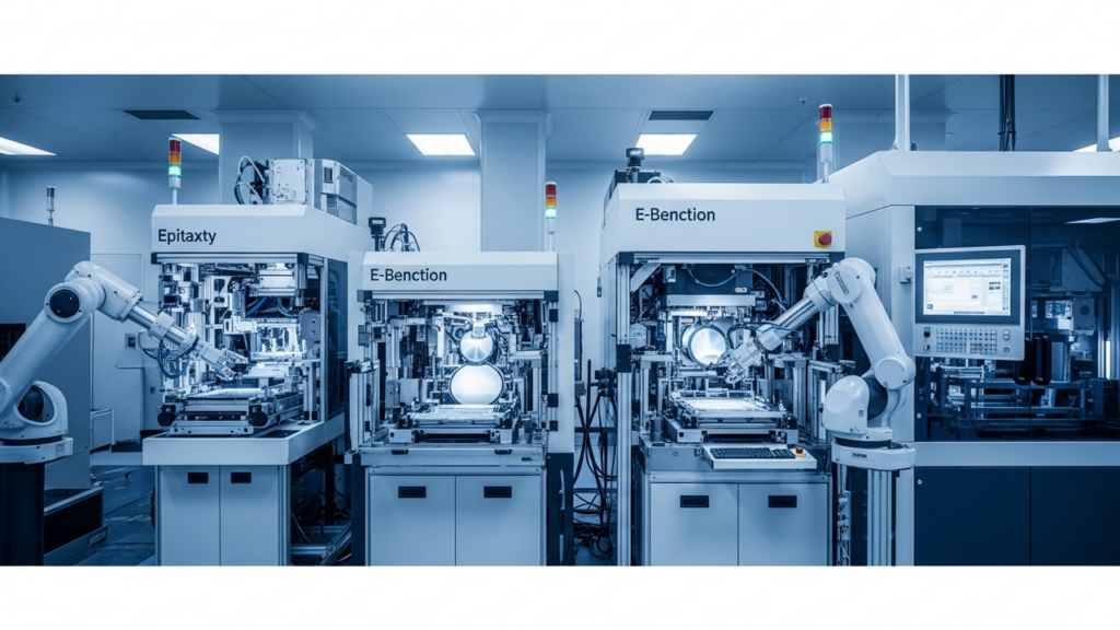
Applied Materials Unveils New Systems for DRAM and Advanced Packaging to Accelerate AI Chip Manufacturing, Featuring Epitaxy, CMP, and E-beam Inspection Technologies
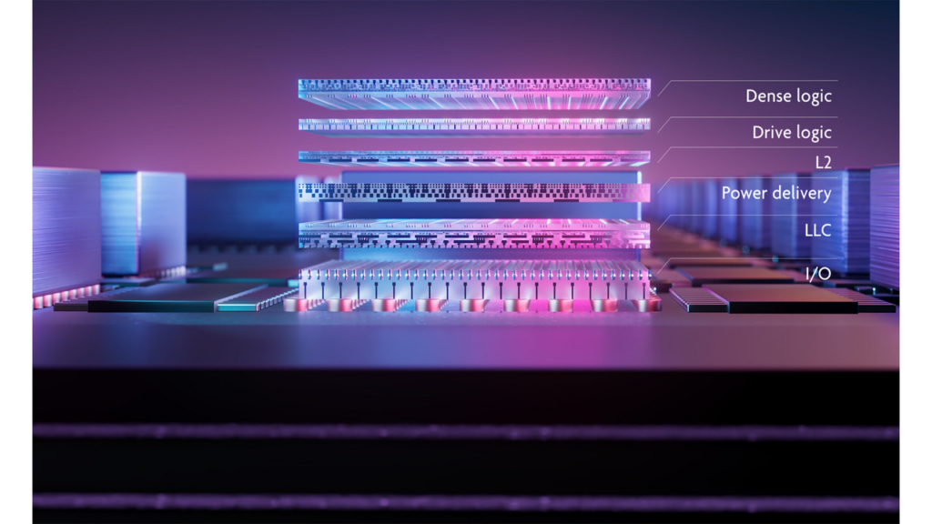
Barchart.com USA Overview Applied Materials has introduced a suite of new chipmaking systems designed to accelerate the construction of advanced 3D chip architectures powering next-generation AI. This includes epitaxy systems optimizing ... -
Applied Materials Unveils New Systems to Accelerate DRAM and Advanced Packaging for AI Chips
Applied Materials, Inc. USA Overview Applied Materials has introduced a suite of new material engineering systems designed to accelerate the manufacturing of advanced 3D chip architectures crucial for next-generation AI. These innovation... -
Intel and Tesla Partner on AI6 Data Centers, Tapping Advanced Packaging for Production at Austin’s ‘Terafab’
Jamie's Substack USA Overview Tesla has announced a strategic partnership with Intel Foundry Services to scale its AI6 chip-powered data center clusters, extensively utilizing Intel's advanced packaging technologies. The collaboration wi... -
Imec and EV Group Set New World Record for 3D Chip Stacking Precision with Sub-40nm Wafer Bond Overlay
PR Newswire ベルギー Overview Imec and EV Group have achieved a world-record post-bond overlay accuracy of less than 40 nanometers across a 300mm wafer for 200nm pitch hybrid bonding, a crucial advancement for next-generation 3D ICs. Dem... -
KLA’s Advanced Packaging Business Soars, Projecting Over $1.3B Revenue in FY2026 Driven by AI Inspection Demand
Bitget USA Overview KLA Corporation, a global leader in semiconductor process control and yield management, is experiencing rapid growth in its advanced packaging business, driven by the increasing complexity of AI chips. Revenue from th... -
TSMC Unveils SoIC 3D Stacking Roadmap: Achieving 4.5µm Pitch by 2029, Enabling Face-to-Face Chiplet Integration for Fujitsu Monaka CPU
専門メディア Taiwan Overview TSMC has revealed its SoIC (System on Integrated Chips) 3D stacking roadmap, targeting a 4.5-micron pitch by 2029, down from today's 6 microns. This advanced face-to-face (F2F) chiplet stacking technology, pa...




12