DRAM– tag –
-

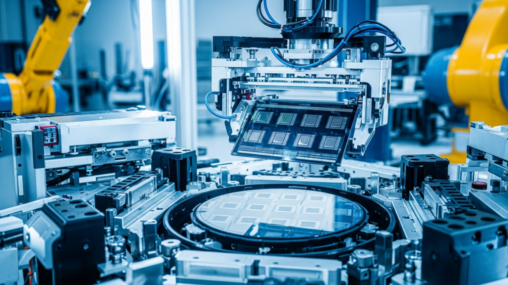
Applied Materials Unleashes Six New Systems to Turbocharge AI Chips with Advanced Packaging and Sub-10nm Defect Detection
Applied Materials USA Overview Applied Materials has launched six innovative systems to significantly accelerate the development and manufacturing of DRAM and advanced packaging for next-generation AI chips. These solutions tackle critic... -
SK Hynix Announces Massive $64 Billion Investment in South Korea to Bolster AI Memory and Packaging Capabilities
Biggo Finance South Korea Overview SK Hynix has unveiled plans for a colossal $64 billion investment in memory chip and advanced packaging facilities within South Korea over the coming years. This strategic outlay aims to address the soa... -
Applied Materials Unveils New Systems to Propel DRAM & Advanced Packaging for AI Chips
StockTitan USA Overview Applied Materials has introduced a suite of new systems designed to dramatically enhance DRAM and advanced packaging processes, directly addressing the escalating performance demands of AI chips. These innovations... -
SK hynix’s Early Strategic Investment in AI and HBM Drives Market Value Lead Over Samsung, Bolstering Production Capacity for NVIDIA Demand
Reuters South Korea Overview SK hynix's early and aggressive investment in HBM (High Bandwidth Memory) technology and significant capacity expansion, anticipating future NVIDIA demand, has allowed it to differentiate from Samsung Electro... -
HBM4E Set to Dominate High-Performance Memory Market by Late 2026-2027 with Up to 4.0 TB/s Single-Stack Bandwidth and 48GB+ Capacity, Accelerating AI Models
Ersa Electronics Global Overview HBM4E is projected to lead the high-performance memory market from late 2026 to 2027, offering a single-stack bandwidth of up to 3.6–4.0 TB/s and capacities exceeding 48GB, significantly boosting ultra-la... -
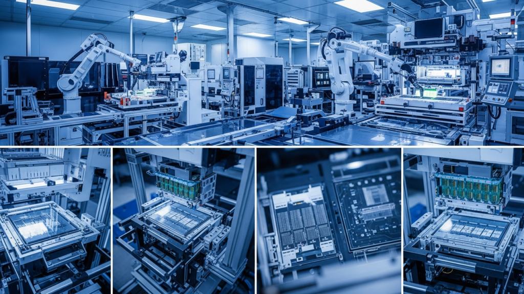
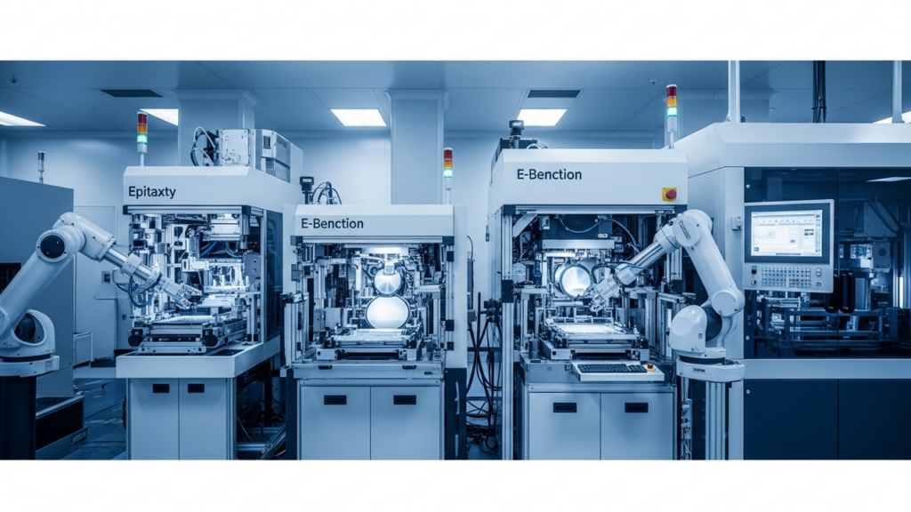
Applied Materials Unveils New Systems for DRAM and Advanced Packaging to Accelerate AI Chip Manufacturing, Featuring Epitaxy, CMP, and E-beam Inspection Technologies
Barchart.com USA Overview Applied Materials has introduced a suite of new chipmaking systems designed to accelerate the construction of advanced 3D chip architectures powering next-generation AI. This includes epitaxy systems optimizing ... -
Imec Unveils Vertically Stacked IGZO FeFETs, Revolutionizing AI Memory Density and Efficiency
IN Electronics & Design ベルギー Overview Imec has achieved a significant breakthrough in ferroelectric memory for AI systems, demonstrating a vertically stacked FeFET architecture utilizing IGZO and successfully reducing ferroelectric c... -
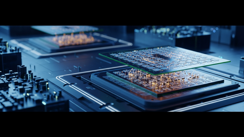
Applied Materials Unveils New Systems to Accelerate DRAM and Advanced Packaging for AI Chips
Applied Materials, Inc. USA Overview Applied Materials has introduced a suite of new material engineering systems designed to accelerate the manufacturing of advanced 3D chip architectures crucial for next-generation AI. These innovation... -
SK hynix Begins Shipping Next-Gen HBM4E AI Memory Chips with 12-Layer Stack, 48GB Capacity, 16Gbps per Pin, and Over 20% Power Efficiency Boost
Bisinfotech South Korea Overview SK hynix has commenced shipments of its next-generation HBM4E AI memory chips, featuring a 12-layer stack with 48GB capacity, ultra-fast data transfer rates of up to 16Gbps per pin, and over 20% improved ... -
Samsung Considers New HBM-Focused Advanced Semiconductor Packaging Plant in South Korea’s Honam Region to Meet AI Server Demand
SamMobile South Korea Overview Samsung Electronics is exploring the construction of a new advanced semiconductor packaging facility in South Korea's Honam region, with Gwangju emerging as a prime candidate. This project aims to bolster S...