Hybrid Bonding– tag –
-

HBM4 Competition Shifts to Cooling Technology Amid Hybrid Bonding Delays and Nvidia’s Next-Gen GPU Trends
DigiTimes Taiwan Overview Industry experts note that the focus of competition in the 6th-generation High-Bandwidth Memory (HBM4) market is shifting towards cooling technology, against the backdrop of delays in hybrid bonding adoption. HB... -
Indian State of Madhya Pradesh Signs MoU for ₹6,200 Crore OSAT Facility with Paras Semiconductors, Advancing Heterogeneous Integration and 3D Packaging
ET Government India Overview The government of Madhya Pradesh, India, announced a Memorandum of Understanding with Paras Semiconductors to establish an advanced semiconductor packaging OSAT (Outsourced Semiconductor Assembly and Test) fa... -
Samsung Delays Hybrid Bonding HBM Mass Production to 2029-2030, Aligning with Technical Challenges and NVIDIA’s Next-Gen GPUs
TrendForce South Korea Overview Samsung Electronics is reportedly delaying the full-scale mass production of its hybrid bonding technology for next-generation HBM and logic semiconductors until 2029-2030. The company is currently buildin... -
Besi Semiconductor Reports Doubled Quarterly Orders Driven by Soaring AI and Hybrid Bonding Demand, Expanding Customer Base
WHTC (Reuters) Netherlands Overview BE Semiconductor Industries (Besi) announced a more than twofold increase in quarterly orders year-over-year, driven by robust demand from AI, hybrid bonding, photonics, and data centers. The company's... -
Samsung Electronics Advances “2.xD” Packaging Integrating HBM, Logic, and Optical Tech to Resolve AI Power and Heat Bottlenecks
BigGo Finance South Korea Overview Samsung Electronics is developing "2.xD" next-generation packaging technology that integrates High Bandwidth Memory (HBM), logic chips, and silicon photonics (SiPh) into a single package to address crit... -
Applied Materials’ Material Engineering Innovations, Led by Hybrid Bonding, Key to Scaling AI Chip Performance in the AI Era
Applied Materials (Official Blog/Article) USA Overview Applied Materials emphasizes that material engineering innovations, including its Kinex hybrid bonding system, are critical for scaling AI chip performance. The company is advancing ... -
Applied Materials Unveils Seven New Systems for AI Chip DRAM Performance and Advanced 3D Packaging, Accelerating Bottleneck Resolution
Industry News International Overview Applied Materials introduced seven new semiconductor manufacturing systems designed to address bottlenecks in AI chip production, specifically enhancing DRAM performance scaling and advanced 3D packag... -
IDTechEx Analyzes Materials Shaping the Future of Advanced Semiconductor Packaging, Including 2.5D/3D Cu-Cu Hybrid Bonding and Glass Panel-Based Technologies
IDTechEx UK Overview This article is an overview of a market research report published by IDTechEx. IDTechEx's latest report focuses on materials shaping the future of advanced semiconductor packaging, including 2.5D and 3D Cu-Cu hybrid ... -
Semiconductor Industry Pivots to Heterogeneous Large-Scale Integration (HLSI) as AI Reshapes Chip Design
Next Move Strategy Consulting (via EE Times) USA Overview Driven by surging AI workloads, the semiconductor industry is dramatically shifting beyond traditional System-on-Chip (SoC) paradigms towards Heterogeneous Large-Scale Integration... -
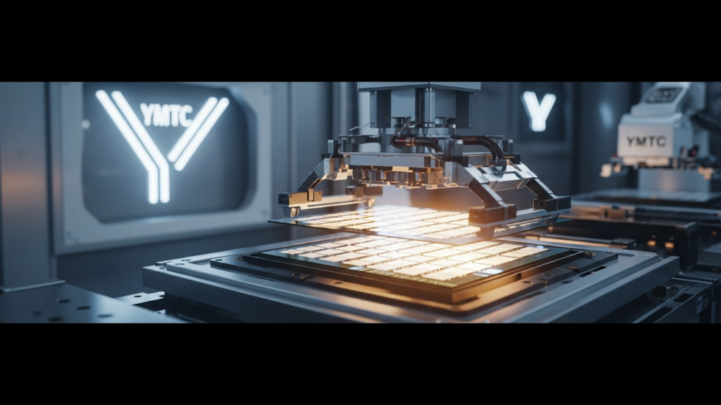
China’s Memory Industry Accelerates HBM3/3E Development; YMTC Leads in Wafer-to-Wafer Hybrid Bonding Patents
BloomingBit.io China Overview China's memory industry is rapidly advancing, with companies like CXMT focusing on HBM3 and HBM3E development, thereby narrowing the technology gap with South Korea. Notably, Yangtze Memory Technologies Co. ...