Hybrid Bonding– tag –
-

IDTechEx Analyzes New 2.5D/3D Semiconductor Packaging Trends: Glass Interposers and Hybrid Bonding Drive Evolution
IDTechEx UK Overview IDTechEx's analysis highlights glass interposers and hybrid bonding as critical emerging trends in semiconductor packaging. Glass interposers offer compatibility with panel-level packaging, promising cost-effective, ... -
ECTC 2026 Highlights Advanced Packaging Future: Glass Substrates and FOPLP at the Core of System Innovation
Advanced Packaging Magazine USA Overview ECTC 2026 emphasized a structural shift in semiconductor innovation, moving beyond transistor scaling to packaging and integration technologies. Noteworthy advancements in heterogeneous integratio... -
JEDEC Relaxes HBM4 Package Height to 775 µm, Enabling 12-Hi/16-Hi Stacks Without Immediate Cu-Cu Hybrid Bonding
Exponential Industry USA Overview JEDEC has relaxed the HBM4 package height specification from 720 µm to 775 µm, allowing for 12-Hi and 16-Hi stack HBM modules without immediate reliance on Cu-Cu hybrid bonding. HBM utilizes 3D stacked D... -
KLA Forecasts $1.1 Billion in Advanced Packaging Revenue for 2026, Driven by Surging AI and HBM Demand
Quartz USA Overview KLA Corporation anticipates its advanced packaging business revenue will reach approximately $1.1 billion in 2026, representing over 70% year-over-year growth, fueled by increasing AI infrastructure investments and se... -
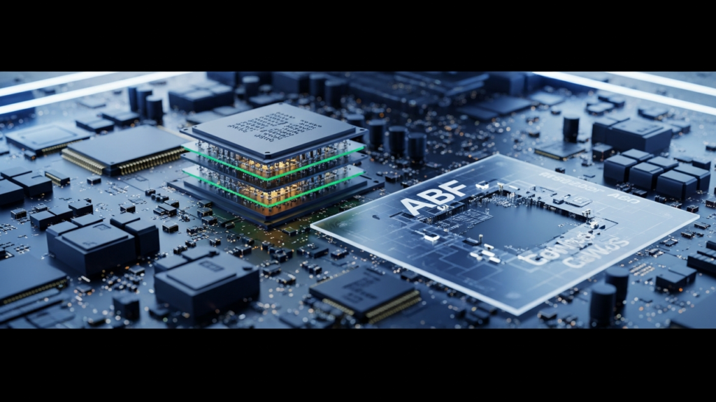
TSMC Achieves Over 98% CoWoS Yield; ABF Substrates Emerge as Next Bottleneck for AI Chip Expansion
Xenospectrum Taiwan Overview TSMC has announced that its advanced CoWoS packaging technology, particularly for 5.5x reticle AI chip products, consistently achieves yields exceeding 98%. While CoWoS capacity has doubled annually for three... -
IMAPS Device Packaging Conference 2026 PDCs Focus on Advanced Packaging for Chiplets and Heterogeneous Integration, Highlighting Hybrid Bonding
IMAPS USA Overview IMAPS Device Packaging Conference 2026 Professional Development Courses (PDCs) extensively covered "Advanced Packaging for Chiplets and Heterogeneous Integration." The courses defined various 2D to 3.5D IC integrations... -
ECTC2026 Unveils Future of Semiconductor Packaging: Precision Adhesives and Low-Temperature Hybrid Bonding for HBM Integration
Tech I Japan Overview ECTC2026 highlighted critical R&D in advanced semiconductor packaging, showcasing innovations in chiplet integration, hybrid bonding, and opto-electronic convergence. Key presentations included Mitsui Chemicals ... -
Besi Achieves Record €292.9M Orders in Q2 2026, Driven by AI Demand and 128.8% Growth in Hybrid Bonding Technology
ET Electronics News Netherlands Overview BE Semiconductor Industries (Besi) reported record Q2 2026 orders of €292.9 million, a 128.8% increase year-over-year, primarily fueled by robust AI-related demand and the surging adoption of its ... -
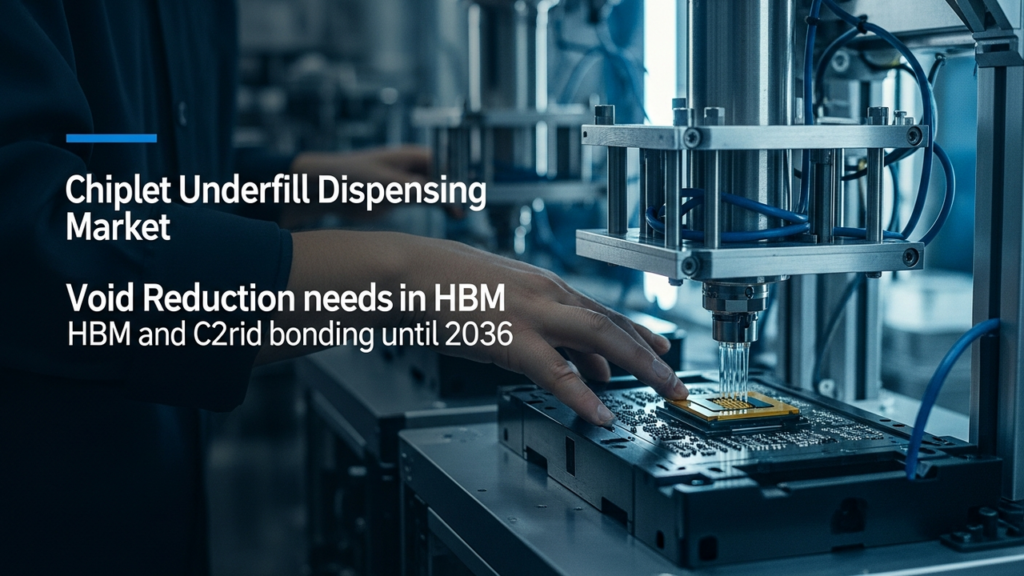
Chiplet Underfill Dispensing Market to Grow Through 2036 Driven by HBM and C2W Hybrid Bonding Void Reduction Needs
Fact.MR USA Overview This article summarizes a market research report from Fact.MR. The chiplet underfill dispensing market is growing, driven by the need for wafer-level underfill in HBM manufacturing and tailored viscosity/cure profile... -
BESI Records All-Time High Orders with 128.8% Y-o-Y Growth Driven by AI Packaging and Hybrid Bonding Demand
BE Semiconductor Industries N.V. Netherlands Overview BE Semiconductor Industries (BESI), a Dutch equipment manufacturer, reported a record €292.9 million in orders for Q2 2026, marking a 128.8% year-on-year increase, fueled by strong de...