SK Hynix– tag –
-

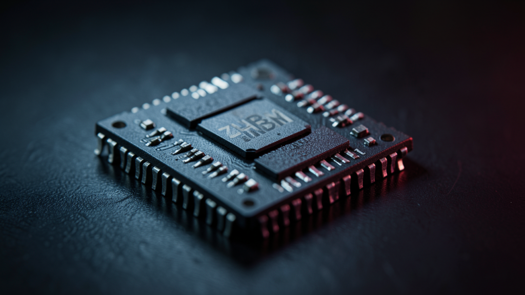
Samsung’s zHBM Concept Promises 70% Lower I/O Power, 2.3x Bandwidth vs. HBM5 via Hybrid Bonding for Edge AI
Tom's Hardware South Korea Overview Samsung proposes zHBM, an innovative memory architecture that directly stacks DRAM onto the processor, bypassing the interposer, and is projected to reduce I/O power by approximately 70% compared to HB... -
Samsung Electronics Reorganizes Cheonan Plant for HBM Packaging, Outsourcing Mobile AP Backend Processes to Boost AI Memory Capacity
TrendForce South Korea Overview Samsung Electronics is reportedly reorganizing its Cheonan plant's backend operations to prioritize High Bandwidth Memory (HBM) packaging due to surging AI demand. This strategic shift involves phasing out... -
Korea and Taiwan Surge as Semiconductor Equipment Investment Hubs, Driven by HBM and Advanced Packaging in H1 2026
The Information Network USA, South Korea, Taiwan Overview In the first half of 2026, global semiconductor equipment sales witnessed a significant geographical pivot, with South Korea (up 32.4%) and Taiwan (up 24.0%) emerging as primary g... -
South Korea Accelerates Advanced Packaging Investments, Establishing Itself as Core of Global AI Semiconductor Supply Chain
Investment Monitor South Korea, USA Overview South Korea is significantly boosting its advanced packaging investments to meet surging AI semiconductor export demand. SK Hynix plans to complete a ₩19 trillion ($12.9 billion) advanced pack... -
Samsung Dedicates Half of Its 4nm Foundry Capacity to HBM4 Base Dies Amid AI Boom
ZDNet Korea South Korea Overview Samsung Electronics is reportedly allocating over 50% of its advanced 4nm foundry capacity—specifically 15,000 wafers per month out of an estimated 30,000 total—to the production of HBM4 base dies. This s... -
Micron Reportedly Targets Doubling HBM Capacity to 100,000 Wafers/Month by End-2026, Boosting 12-High HBM4 for NVIDIA Vera Rubin
digitimes USA Overview Micron is reportedly targeting a near-doubling of its High Bandwidth Memory (HBM) production capacity to approximately 100,000 wafers per month by the end of 2026. This significant expansion focuses on ramping up p... -
Samsung Electronics Establishes Advanced Packaging R&D Center in Yokohama to Deepen Collaboration with Japanese Suppliers for HBM Technologies
digitimes South Korea Overview Samsung Electronics has opened an advanced packaging research center in Yokohama, Japan, to strengthen development cooperation with Japanese suppliers of critical materials and equipment for HBM. This strat... -
NVIDIA to Boost CoWoS Production Capacity by 3.5x to Over 120,000 Wafers/Month by End-2026, Securing HBM4 Supply
SemiconductorX USA Overview NVIDIA plans to scale its CoWoS (Chip-on-Wafer-on-Substrate) production capacity by 3.5x to 120,000–130,000 wafers per month by the end of 2026, up from 35,000, driven largely by its own demand. The company is... -
Intel’s EMIB-T Advanced Packaging Projected for Significant Contribution by 2029 as CoWoS Constraints Drive Google’s Interest
TrendForce Taiwan Overview Intel's EMIB (Embedded Multi-die Interconnect Bridge) technology, particularly EMIB-T, is attracting strong interest from major tech firms like Google amid persistent TSMC CoWoS supply constraints. Intel projec... -
AI Supply Chain Maxed Out: 40-Week Lead Times Become New Normal as HBM Emerges as Primary Bottleneck Over TSMC CoWoS
Markets Insider USA Overview The AI supply chain faces severe constraints, with 40-week lead times becoming the new norm. High Bandwidth Memory (HBM) has replaced TSMC's CoWoS advanced packaging as the primary bottleneck, driven by NVIDI...