Wafer Level Packaging– tag –
-

Fraunhofer IPMS Develops High-Density Chiplet Systems at Wafer Level, Advancing Integration for AI and HPC
Design And Reuse Germany Overview Fraunhofer IPMS has developed high-density chiplet systems at the wafer level, aiming to enhance integration for AI and high-performance computing (HPC) applications. This research contributes to the min... -
KLA’s Advanced Packaging Business Soars, Projecting Over $1.3B Revenue in FY2026 Driven by AI Inspection Demand
Bitget USA Overview KLA Corporation, a global leader in semiconductor process control and yield management, is experiencing rapid growth in its advanced packaging business, driven by the increasing complexity of AI chips. Revenue from th... -
ASE Unveils Industry-First Automated 310mm Panel-Level Packaging Line for AI and Chiplet Integration
AnySilicon Taiwan Overview Advanced Semiconductor Engineering (ASE) has developed an automated 310mm x 310mm panel-level packaging (PLP) production line, a significant advancement for AI processors and chiplet architectures. This industr... -
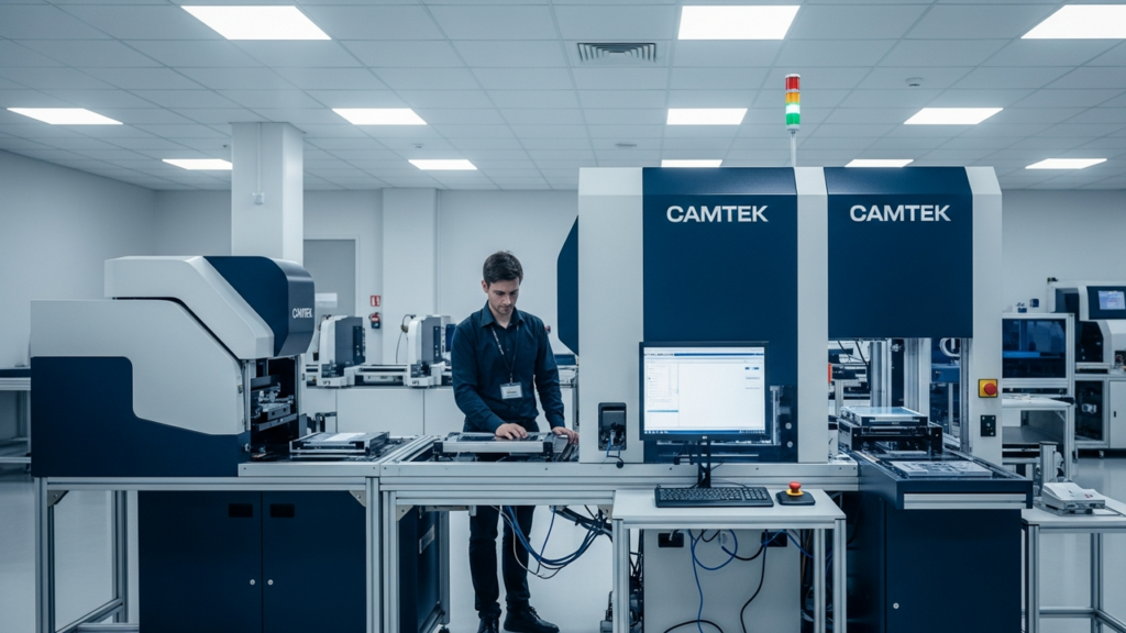
Camtek’s Precision Inspection and Metrology Solutions Drive Yield and Efficiency in Advanced Packaging
Camtek イスラエル Overview Camtek provides industry-leading 2D and 3D inspection and metrology platforms that address the escalating complexity and rapid growth of the advanced packaging market. Featuring sub-micron defect detection, CAD... -
KLA Enhances AI Chip Production with Comprehensive Wafer Inspection and Metrology for Advanced Packaging
KLA USA Overview KLA offers comprehensive inspection and metrology solutions for complex advanced wafer-level packaging processes, including 2.5D/3D integration, WLCSP, and FOWLP. Its AI-powered systems improve yield, defect detection, a...