Key Findings
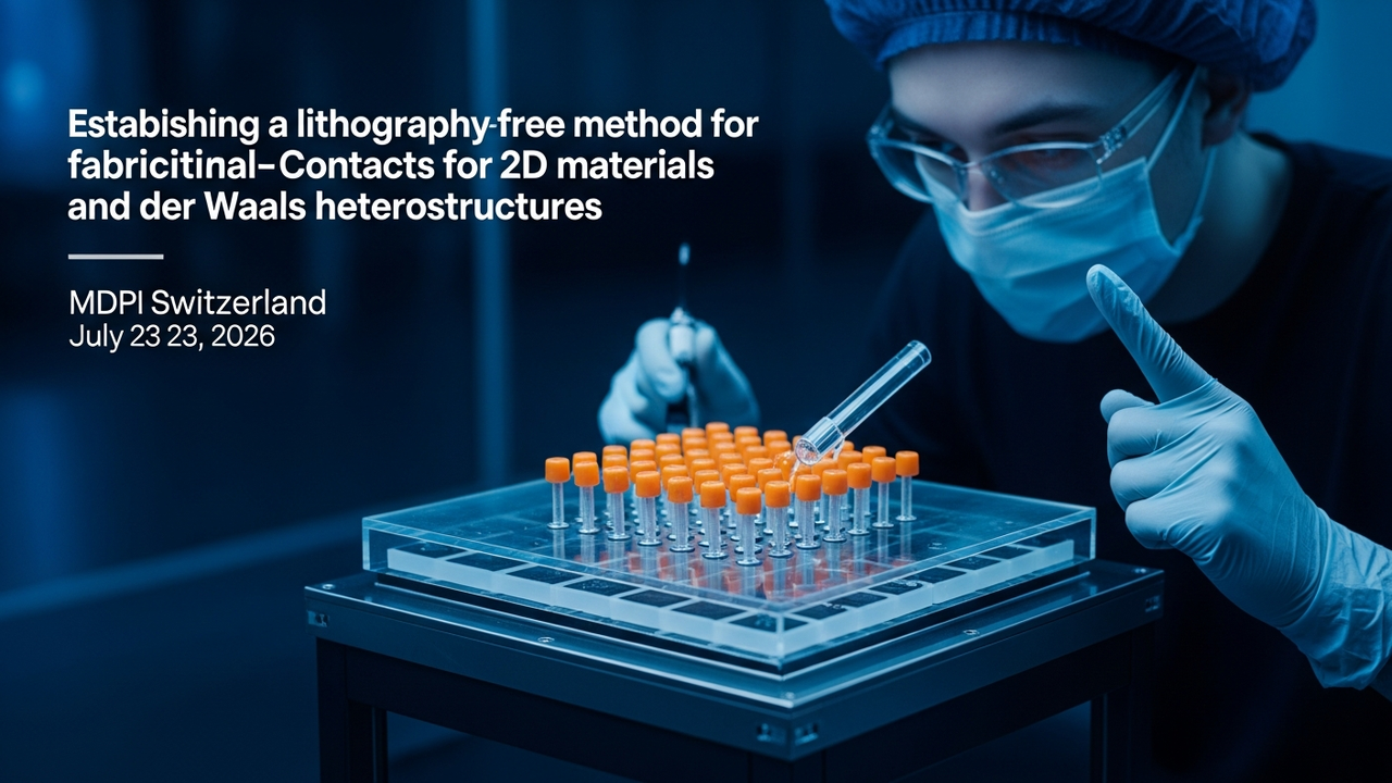
This research successfully established silver paint micromanipulation (SPMM) as a novel lithography-free method for creating electrical contacts for 2D materials and van der Waals heterostructures. This technology holds significant potential to reduce dependence on costly cleanroom facilities and drastically cut down device development time and cost.
Technical / Clinical Details
Conventional 2D material device fabrication has historically relied on complex and expensive cleanroom processes, such as photolithography and electron beam lithography, demanding considerable time and specialized expertise. SPMM offers an additive, room-temperature approach where fine silver paint is directly applied onto the surface of 2D materials using a micromanipulator to form electrical contacts. This process effectively bypasses the corrosive chemical solvents and high-temperature treatments commonly used in traditional processes, which can cause thermal damage to delicate materials. The research team applied SPMM to multilayer graphene and molybdenum disulfide (MoS2) field-effect transistors (FETs) and evaluated their performance. The fabricated devices exhibited linear Ohmic behavior, confirming excellent electrical contact properties. Furthermore, these devices demonstrated environmental stability, maintaining reliable operation over extended periods. For optoelectronic devices, they showed high responsivity, suggesting promising applications in photodetectors and flexible displays.
Background & Context
2D materials like graphene and MoS2 have garnered significant attention due to their exceptional electrical and optical properties, which promise to enable next-generation high-speed, low-power electronic devices and flexible electronics. However, realizing the full potential of these materials has been hampered by the lack of simple and efficient techniques for creating high-quality electrical contacts. The complexity and cost of conventional manufacturing processes have been one of the primary barriers to the commercialization of 2D materials. SPMM addresses this bottleneck, opening the door for more researchers and companies to access 2D material device development.
Strategic Significance & Outlook
SPMM technology will serve as a powerful tool to accelerate 2D material-based prototype development, aiding the transition from lab-scale ideas to commercial products. Future efforts will focus on developing automated techniques to further improve SPMM resolution and reproducibility, as well as validating its applicability to a wider range of 2D materials and device structures. Applications are anticipated across various fields, including flexible electronics, wearable devices, and IoT sensors, which are expected to contribute significantly to the widespread adoption and practical use of 2D material technology. This represents a crucial step in building a new paradigm for device manufacturing through the convergence of materials science and electrical engineering.
Source: https://www.mdpi.com/2072-666X/17/7/844
Get our weekly technology intelligence — free
Receive an infographic that lets you judge at a glance whether each field’s analysis report is worth reading.
Subscribe Free — Weekly Tech Intelligence
By subscribing, you’ll receive Troy-Technical’s weekly technology intelligence newsletter.
- Your email and selected fields are used only to deliver the newsletter.
- We never share your information with third parties.
- You can unsubscribe anytime via the link in each email.
See our Privacy Policy for details.
Takes about a minute · Unsubscribe anytime





Comments