


Key Findings
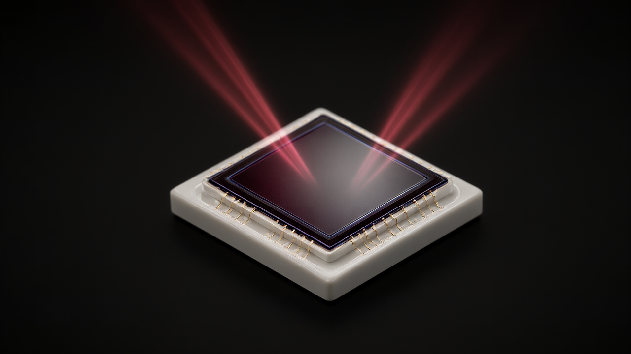
Tanaka Precious Metals, in collaboration with Nagoya University’s Torimoto Laboratory, has developed a lead-free noble metal quantum dot material responsive to near-infrared light. When implemented as a light-sensing layer in a simple optical sensor, the material achieved a maximum external quantum efficiency (EQE) of 18.4% within the short-wave infrared (SWIR) wavelength range of 1200 to 1700 nm.
Technical Details
The developed material is a compound semiconductor quantum dot composed primarily of silver, sulfur, and tellurium (Ag-S-Te). Unlike previous alternatives, it contains neither lead (Pb) nor cadmium (Cd), ensuring compliance with EU RoHS directives. Technical advantages include:
- Manufacturing: The material can be produced via printing processes, eliminating the need for vacuum processes.
- Cost: Sensor manufacturing costs are estimated to be approximately one-tenth those of indium gallium arsenide (InGaAs).
- Customization: The joint research focused on composition control, particle size control, and surface modification to allow for customized optical properties.
- Sustainability: Tanaka Precious Metals intends to apply its noble metal recycling technology to recover and refine precious metals from manufacturing scraps and used samples to reduce initial and running costs.
Background and Context
Infrared sensing is critical for 3D sensing, facial recognition, LiDAR, and biological sensing. While InGaAs has been the industry standard, it faces challenges regarding complex manufacturing, high costs, and the limited supply of indium. Lead sulfide (PbS) quantum dots were considered as alternatives, but their lead content restricted their use in consumer electronics due to RoHS regulations.
Significance and Outlook
The 1200–1700 nm waveband is less susceptible to solar noise and adverse weather, enabling high-precision outdoor sensing. Potential applications include automotive LiDAR, smartphone facial recognition, industrial inspection cameras, and wearable devices. The material will be presented at “Okinawa Colloids” (November 1–6, 2026) and the “Nanotech 26th International Nanotechnology Exhibition and Conference” (December 16–18, 2026), with sample provision scheduled to begin in January 2027.
Source: https://response.jp/article/2026/10/28/418316.html
Get our weekly technology intelligence — free
Receive an infographic that lets you judge at a glance whether each field’s analysis report is worth reading.
Subscribe Free — Weekly Tech Intelligence
By subscribing, you’ll receive Troy-Technical’s weekly technology intelligence newsletter.
- Your email and selected fields are used only to deliver the newsletter.
- We never share your information with third parties.
- You can unsubscribe anytime via the link in each email.
See our Privacy Policy for details.
Takes about a minute · Unsubscribe anytime