Key Findings
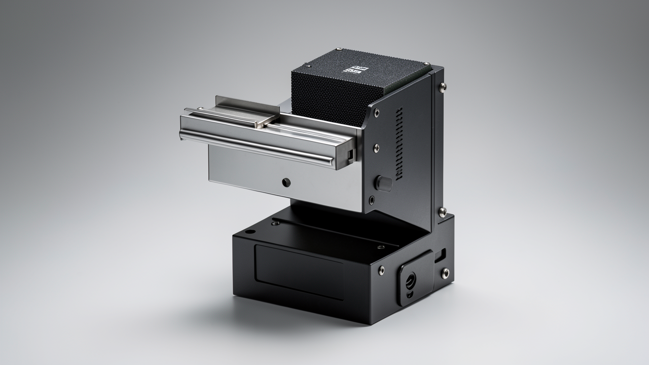
The adoption of PEEK (Polyether Ether Ketone), a high-performance polymer, is rapidly accelerating within the semiconductor manufacturing equipment sector. PEEK is recognized as an ideal material for critical components such as wafer handling arms, vacuum insulators, and valve seats, owing to its unparalleled purity, superior thermal performance, robust chemical resistance, exceptional dimensional stability, and versatile processability. This widespread integration of PEEK is instrumental in resolving long-standing issues associated with traditional materials, including particle generation, chemical contamination, and thermal expansion, thereby dramatically enhancing the efficiency and reliability of semiconductor manufacturing processes.
Technical / Clinical Details
Semiconductor manufacturing demands extremely clean environments and precise process control. Conventional metallic materials and general plastics have historically presented challenges such as micro-particle generation, metal ion leaching, or vulnerability to specific chemicals. PEEK addresses these issues through its distinct properties: Firstly, its **high purity** minimizes the risk of trace contaminant adhesion to wafer surfaces. Secondly, **superior thermal performance** (continuous use temperature above 250°C) prevents component deformation and degradation, maintaining dimensional stability even in high-temperature process environments. Furthermore, PEEK’s **resistance to a wide range of chemicals**, including acids, bases, and organic solvents, eliminates concerns about material degradation or dissolution during various cleaning and etching processes. Its **high mechanical strength and rigidity** prevent deflection during high-speed wafer handling, enabling precise positioning. Additionally, **low moisture absorption** and a **low coefficient of thermal expansion** guarantee precise dimensional stability and suppress component deformation due to temperature fluctuations. These combined properties make PEEK crucial for wafer carriers, Chemical Mechanical Planarization (CMP) rings, test sockets, ion implantation components, gaskets, and seals across various stages of semiconductor manufacturing processes.
Background & Context
The semiconductor industry is experiencing unprecedented acceleration in speed and integration, driven by megatrends such as AI, 5G, IoT, and automotive electrification. Consequently, semiconductor manufacturing equipment faces increasingly stringent performance and reliability requirements. Specifically, preventing contamination during processes, adapting to high-temperature environments, and achieving high-precision component handling are directly linked to chip yield and production efficiency, making material selection critically important. The shift towards high-performance polymers like PEEK is not merely a material substitution but a strategic move supporting the evolution of the entire semiconductor manufacturing process. This contributes to reducing manufacturing costs, extending equipment lifespan, and accelerating the development of next-generation semiconductors.
Strategic Significance & Outlook
The application of PEEK in semiconductor manufacturing equipment is expected to expand even further. Manufacturers will likely focus on developing specialized PEEK grades tailored for specific process requirements, such as ESD (Electrostatic Discharge) protection, plasma resistance, and even higher temperature tolerance, or incorporating PEEK into composite materials. Furthermore, the combination of PEEK with 3D printing technologies holds the potential for more rapid and cost-effective manufacturing of complex PEEK components. The integration of high-performance polymers like PEEK with precision manufacturing technologies is expected to further accelerate innovation in the global semiconductor industry and enhance its competitiveness. This exemplifies how material technology forms the core support for the development of next-generation electronics.
Get our weekly technology intelligence — free
Receive an infographic that lets you judge at a glance whether each field’s analysis report is worth reading.
Subscribe Free — Weekly Tech Intelligence
By subscribing, you’ll receive Troy-Technical’s weekly technology intelligence newsletter.
- Your email and selected fields are used only to deliver the newsletter.
- We never share your information with third parties.
- You can unsubscribe anytime via the link in each email.
See our Privacy Policy for details.
Takes about a minute · Unsubscribe anytime









Comments