


Key Findings
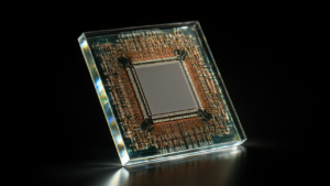
Intel is transitioning its advanced packaging from high-end processor support to a core strategy for the AI chip market. The company targets 12x reticle-size SiPs on 120×180mm packages by 2028, utilizing glass-core substrates for improved stability and lower warpage. CEO Lip-Bu Tan noted during the August 2026 earnings call that customer interest in EMIB-T is very high, with production capacity ramping planned for 2027.
Technical Details: EMIB and Foveros
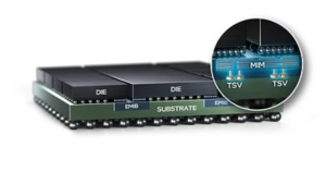
The EMIB (Embedded Multi-die Interconnect Bridge) roadmap focuses on shrinking interconnect pitches from 55 microns to 45, then 36, and eventually 25 microns. Functional iterations include EMIB-M, which integrates metal-insulator-metal (MIM) capacitors, and EMIB-T, which employs through-silicon vias (TSVs) for vertical power delivery to support HBM4-class memory and multi-kilowatt SiPs.
The Foveros family is positioned against TSMC’s CoWoS with three 2.5D variants:
- Foveros-S: Uses a silicon interposer; currently supports up to 4x reticle size.
- Foveros-R: Uses fan-out redistribution layer (RDL) technology; mass production planned for 2027.
- Foveros-B: Combines RDL with localized silicon bridges.
These variants target sub-25-micron pitches and bump densities increasing from 772 to 1,600 connections per square millimeter, with interconnect power of 0.15 pJ/bit.
Foveros Direct 3D and Hybrid Bonding
Foveros Direct 3D replaces solder with copper-to-copper hybrid bonding, achieving interconnect pitches below 10 microns. This technology enables densities up to 10,000 connections per square millimeter and reduces interconnect power to below 0.05 pJ/bit. The Xeon 6+ “Clearwater Forest” processor is the first mass-produced product to utilize this bonding for Intel 18A compute dies.
Significance and Outlook
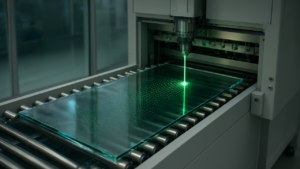
By evolving toward finer pitches and larger package sizes, Intel aims to capture spillover orders resulting from TSMC’s CoWoS supply constraints. The move toward glass substrates and hybrid bonding is critical for reducing latency and improving heat dissipation in vertically stacked logic circuits.
Source: https://finance.biggo.com/news/03f6f05f-928f-44ea-a48e-4414bad68127
Get our weekly technology intelligence — free
Receive an infographic that lets you judge at a glance whether each field’s analysis report is worth reading.
Subscribe Free — Weekly Tech Intelligence
By subscribing, you’ll receive Troy-Technical’s weekly technology intelligence newsletter.
- Your email and selected fields are used only to deliver the newsletter.
- We never share your information with third parties.
- You can unsubscribe anytime via the link in each email.
See our Privacy Policy for details.
Takes about a minute · Unsubscribe anytime