
Key Findings
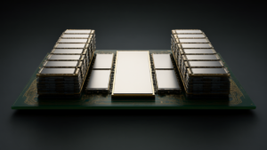
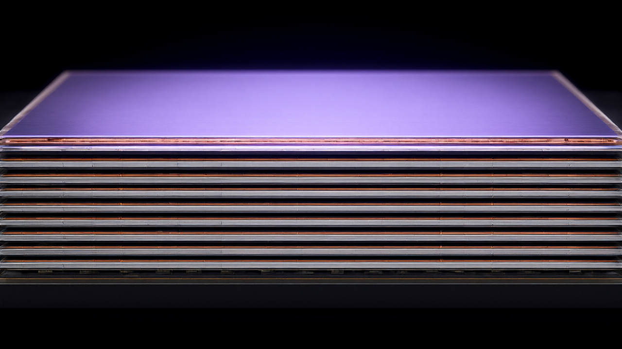
Micron is targeting 2028 for the mass production of the first generation of vHBM, which stacks memory on compute chips, and vEIM, designed for AI inference on edge devices. To achieve this, the company is pursuing a dual-track strategy: shrinking DRAM memory cells while simultaneously advancing packaging technologies to shorten data paths between memory and compute chips.
Technical Details
Micron’s roadmap outlines a progression of manufacturing generations:
- 1γ (1-gamma): Current production generation utilizing EUV lithography.
- 1δ (1-delta): Planned for volume ramp-up in the second half of 2027, targeting a bit-density improvement in the mid-20% range over 1γ. This will serve as the foundation for HBM5, vHBM, and vEIM.
- 1ε (1-epsilon): Under development; planned introduction of wafer bonding.
- ζÅ: Early development stage; planned adoption of High-NA EUV lithography (increasing numerical aperture from 0.33 to 0.55).
- ηÅ: Technology exploration stage; focused on new materials.
Background & Context
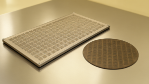
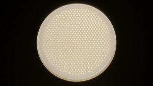
Micron has decided to skip the 4F² cell architecture, despite 20 years of research, citing excessive complexity and cost. Instead, the company will continue improving the existing 6F² cell and developing 3D DRAM. Regarding peripheral circuits, Micron is exploring wafer bonding to decouple the manufacturing of memory cells and peripheral circuits. This approach addresses the constraint where peripheral circuits must otherwise withstand high-temperature heat treatments (550–600°C) required for memory cell fabrication.
Significance & Outlook
By separating the production of peripheral circuits and memory cells via wafer bonding, Micron seeks to optimize manufacturing conditions for each component and improve overall performance. While High-NA EUV improves resolution to form finer patterns, wafer bonding addresses the physical arrangement and scaling of circuits. These combined efforts aim to extend conventional DRAM scaling and restructure memory architecture specifically for AI workloads.
Source: https://xenospectrum.com/en/micron-dram-bonding-vertical-memory/
Get our weekly technology intelligence — free
Receive an infographic that lets you judge at a glance whether each field’s analysis report is worth reading.
Subscribe Free — Weekly Tech Intelligence
By subscribing, you’ll receive Troy-Technical’s weekly technology intelligence newsletter.
- Your email and selected fields are used only to deliver the newsletter.
- We never share your information with third parties.
- You can unsubscribe anytime via the link in each email.
See our Privacy Policy for details.
Takes about a minute · Unsubscribe anytime