Key Findings
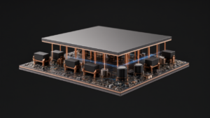
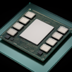
ASE has demonstrated a panel-level packaging (PLP) solution specifically designed for AMD’s next-generation Venice server processors. Initial production is targeted for the first quarter of 2027, likely starting at a limited scale at ASE’s Kaohsiung facility. In a separate development, Taiwan’s Investment Commission approved a $400 million investment by SPIL to establish XCIP TECHNOLOGIES PTE. LTD. in Singapore, a joint venture with Broadcom focused on PLP advanced packaging, assembly, and final testing.
Technical Details
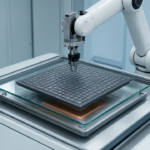
The Venice solution utilizes second-generation Fan-Out Embedded Bridge (FOEB) technology developed through collaboration between ASE, SPIL, and AMD. The technical advantages of transitioning from circular wafers to square panels are as follows:
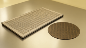
- Substrate Dimensions: ASE uses a 310 x 310 mm square panel.
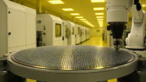
- Capacity Increase: A single panel can accommodate 25 Venice interposers, compared to 22 on a traditional 300 mm circular wafer, representing a 14% increase.
- Scaling Advantage: The advantage of square panels increases with interposer size. For an interposer 9.5 times the reticle size, a panel can hold 9 units, whereas a wafer can only hold 4.
Background & Context
Venice is AMD’s sixth-generation EPYC processor. While AMD previously announced that Venice has begun production ramp-up using TSMC’s 2nm process, the PLP packaging implementation will follow in early 2027. Regarding the Singapore venture, Broadcom is expected to hold a majority stake and lead the facility, while SPIL will handle operations and mass production. This plant focuses on additive fine-line redistribution layer (RDL) technology for PLP substrates, targeting Co-Packaged Optics (CPO) requirements.
Significance & Outlook
The Singapore plant is expected to break ground as early as late 2026, with mass production slated for 2028. The production timelines for ASE and SPIL (2027–2028) align closely with reported plans for TSMC’s CoPoS packaging. This shift toward PLP reflects a strategic move to increase AI chip output and reduce costs as interposer sizes grow.
Source: https://www.blocktempo.com/ase-amd-venice-panel-level-packaging-powertech-broadcom-singapore-plant/
Get our weekly technology intelligence — free
Receive an infographic that lets you judge at a glance whether each field’s analysis report is worth reading.
Subscribe Free — Weekly Tech Intelligence
By subscribing, you’ll receive Troy-Technical’s weekly technology intelligence newsletter.
- Your email and selected fields are used only to deliver the newsletter.
- We never share your information with third parties.
- You can unsubscribe anytime via the link in each email.
See our Privacy Policy for details.
Takes about a minute · Unsubscribe anytime