


Key Findings
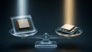
Qualcomm has completed the initial validation of its High Bandwidth Compute (HBC) memory architecture. In testing conducted at its San Diego labs using a 2-layer DRAM sample stack, the company found that HBC delivers more than five times the energy efficiency, measured as bandwidth-per-watt, compared to HBM4.
Technical Details
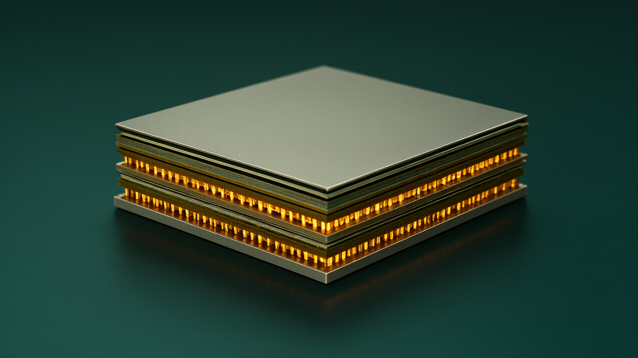
HBC is a near-memory compute architecture that stacks multiple layers of LPDDR5X DRAM dies directly on top of a small compute die. This differs from HBM, which stacks DRAM on a base die connected to a host processor via an ultra-wide memory bus. By placing the compute die at the bottom of the stack, Qualcomm minimizes the distance data must travel, reducing energy consumption.
The architecture offers several technical advantages:
- Cost Reduction: By performing bandwidth-intensive operations on the compute die under the memory, the system requires less bandwidth to connect to the larger processor die. This allows the use of traditional 2D organic substrates instead of expensive advanced packaging like CoWoS or EMIB.
- Capacity: Because HBC utilizes LPDDR5X DRAM dies rather than the thin dies used in HBM, projected capacity is expected to exceed current HBM4 implementations.
- Manufacturing: While the process still requires TSVs to bond DRAM wafers, the complexity is reduced by eliminating the need for high-speed chiplet connectivity.
Background and Context
First introduced during the 2026 Investor Day, HBC is designed to balance memory capacity, performance, and production costs. Qualcomm positions HBC as a superior alternative to HBM, on-die SRAM, and off-package LPDDR by offering better bandwidth than external LPDDR and higher capacity than on-die SRAM without the associated high costs.
Significance and Outlook
The validation of HBC moves the technology toward mass production. The architecture is a central component of the Dragonfly AI250 accelerator and its successors, specifically targeting the memory bandwidth and capacity requirements of AI inference. Commercial product sampling is scheduled to start in 2027, with final shipping products expected to feature 4-layer DRAM stacks.
Get our weekly technology intelligence — free
Receive an infographic that lets you judge at a glance whether each field’s analysis report is worth reading.
Subscribe Free — Weekly Tech Intelligence
By subscribing, you’ll receive Troy-Technical’s weekly technology intelligence newsletter.
- Your email and selected fields are used only to deliver the newsletter.
- We never share your information with third parties.
- You can unsubscribe anytime via the link in each email.
See our Privacy Policy for details.
Takes about a minute · Unsubscribe anytime