HBM– tag –
-

Intel and TSMC Champion Panel-Level Packaging, Projecting a Tenfold Market Expansion
The Elec South Korea Overview Intel and TSMC are aggressively pursuing Panel-Level Packaging (PLP) technology, a move anticipated to expand the associated market tenfold. PLP offers significant production efficiency and cost advantages o... -
ASE to Commence FOPLP Mass Production by End-2026, Launching 15 Expansion Projects Amid AI Chip Boom
TrendForce Taiwan Overview ASE Technology, the world's largest semiconductor packaging and testing services provider, announced plans to begin mass production of Fan-out Panel-Level Packaging (FOPLP) by the end of 2026. This initiative, ... -
Applied Materials Unveils New Systems to Propel DRAM & Advanced Packaging for AI Chips
StockTitan USA Overview Applied Materials has introduced a suite of new systems designed to dramatically enhance DRAM and advanced packaging processes, directly addressing the escalating performance demands of AI chips. These innovations... -
South Korea Pledges $252 Billion for HBM Factories, Meta and xAI Initiate AI Compute Resale Market
Let's Data Science South Korea, USA Overview South Korea has announced a monumental $252 billion investment to support Samsung and SK Hynix in building HBM packaging factories, addressing a critical global AI compute bottleneck. Simultan... -
Henkel Offers Liquid Compression Molding (LCM) Solutions for Wafer-Level and Panel-Level Packaging
Henkel Adhesives Germany Overview Henkel provides encapsulation materials that enable advanced semiconductor packaging technologies where ICs are molded directly on wafers or panels prior to subsequent processing, using Liquid Compressio... -
Resonac’s 2016 Liquid Encapsulant Patent for 2.5D AI Semiconductors Skyrockets in Strategic Value Amid Generative AI Boom
YouTube (3-Min Semi with Tai) Japan Overview Resonac's patent for liquid encapsulants, filed in 2016 for AI semiconductor applications, has dramatically increased in strategic importance with the current generative AI boom. This technolo... -
SK hynix’s Early Strategic Investment in AI and HBM Drives Market Value Lead Over Samsung, Bolstering Production Capacity for NVIDIA Demand
Reuters South Korea Overview SK hynix's early and aggressive investment in HBM (High Bandwidth Memory) technology and significant capacity expansion, anticipating future NVIDIA demand, has allowed it to differentiate from Samsung Electro... -
HBM4E Set to Dominate High-Performance Memory Market by Late 2026-2027 with Up to 4.0 TB/s Single-Stack Bandwidth and 48GB+ Capacity, Accelerating AI Models
Ersa Electronics Global Overview HBM4E is projected to lead the high-performance memory market from late 2026 to 2027, offering a single-stack bandwidth of up to 3.6–4.0 TB/s and capacities exceeding 48GB, significantly boosting ultra-la... -
Applied Materials Unveils New Systems for DRAM and Advanced Packaging to Accelerate AI Chip Manufacturing, Featuring Epitaxy, CMP, and E-beam Inspection Technologies
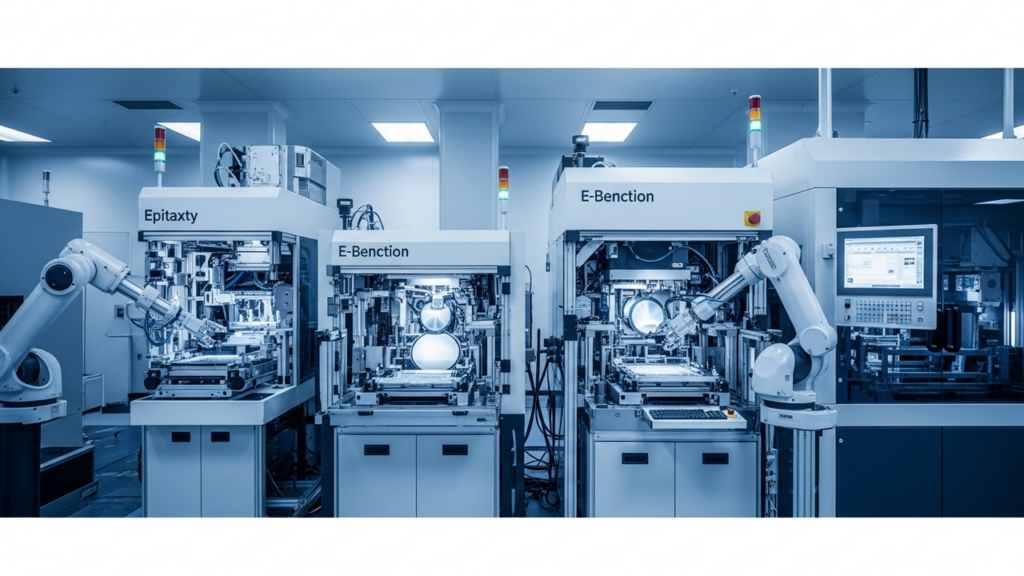
Barchart.com USA Overview Applied Materials has introduced a suite of new chipmaking systems designed to accelerate the construction of advanced 3D chip architectures powering next-generation AI. This includes epitaxy systems optimizing ... -
TSMC’s CoWoS Capacity Dramatically Expands, Eliminating Supply Constraint for NVIDIA B300 Servers and Cutting Lead Times to 8-16 Weeks
Contrary Research Taiwan Overview TSMC's CoWoS (Chip-on-Wafer-on-Substrate) packaging capacity has significantly expanded, effectively resolving a major GPU procurement constraint that had persisted for over six months in 2025. As a resu...