imec– tag –
-

Taiyo Holdings and imec Unveil 700nm 3-Layer RDL Breakthrough for Next-Gen AI Packaging
Quantum Zeitgeist Japan, Belgium Overview Taiyo Holdings, in collaboration with imec, announced at IEEE ESTC 2026 the successful formation of a 3-layer Redistribution Layer (RDL) with a critical dimension of 700 nanometers on 12-inch waf... -
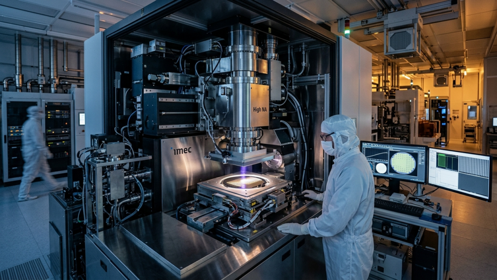
Imec Unlocks 22nm Pitch Single Patterning for High NA EUV Lithography, Accelerating Next-Gen Microchip Manufacturing
imec Belgium Overview Imec has announced a significant advancement in high-NA extreme ultraviolet (EUV) lithography, extending chemically amplified resists to enable single patterning of 22nm pitch line structures. This breakthrough is c... -
Imec Achieves Record 3.8M Junction/cm² Density in Superconducting Circuits with 30nm NbTiN Interconnects, Propelling Next-Gen HPC/AI
imec Belgium Overview Imec has announced a world-first 3-metal-level superconducting circuit featuring NbTiN-based Josephson junctions and ultra-fine 30nm interconnects, achieving an unprecedented density of 3.8 million junctions per squ... -
Industrial Leap: High-Yield GFETs on 200mm Wafers Accelerate Graphene’s CMOS Integration
ACS Publications Belgium Overview A research collaboration, notably involving Imec, has optimized the manufacturing and analysis processes for CMOS-compatible graphene field-effect transistors (GFETs) on 200mm wafers, a critical mileston... -
imec Pioneers Glass Substrates for Next-Gen 3D Packaging, Accelerating AI/HPC Commercialization
EETimes Belgium Overview imec, the renowned Belgian microelectronics research institute, has announced a significant breakthrough in 3D stacked packaging, leveraging glass substrates as interposers. This innovation is pivotal for next-ge... -
IMEC, TSMC, Intel, and Samsung Pursue Atomically-Thin 2D Transistors to Sustain Moore’s Law Beyond Silicon in 2026
Internet Pros USA Overview As silicon transistors approach scaling limits, industry leaders IMEC, TSMC, Intel, and Samsung are shifting to atomically-thin 2D semiconductors for next-generation chips. Materials like molybdenum disulfide (... -
ASML, TSMC, and Imec Achieve Breakthrough 300mm Integration for Industry-Ready 2D-Material Transistors
The cleanroom Portal - Reinraum Online Germany Overview Imec, in collaboration with ASML and TSMC, presented a robust and scalable 300mm integration approach for n- and p-FETs based on 2D materials at the IEEE/JSAP Symposium 2026. This b... -
Imec’s Chiplet Imperative: Analyzing the Transition to High-Bandwidth, Low-Energy AI/HPC Systems
imec ベルギー Overview Imec has published a comprehensive analysis identifying the economic and technical inflection points for transitioning from monolithic ASICs to chiplet-based designs, particularly for AI, HPC, and data center appli... -
Imec Unveils Vertically Stacked IGZO FeFETs, Revolutionizing AI Memory Density and Efficiency
IN Electronics & Design ベルギー Overview Imec has achieved a significant breakthrough in ferroelectric memory for AI systems, demonstrating a vertically stacked FeFET architecture utilizing IGZO and successfully reducing ferroelectric c... -
Imec Targets Optical Interconnect Packaging Bottlenecks for Next-Gen AI and HPC
ApplyKite (imec) ベルギー Overview Imec is seeking a PhD candidate for groundbreaking research into microfluidics and photonics packaging, crucial for optical interconnects in future AI and High-Performance Computing (HPC) systems. The p...



12