Panel Level Packaging– tag –
-

Applied Materials Forecasts Over 70% Growth in Advanced Packaging Revenue, Total Revenue Up 40%, Driven by AI and HBM Demand
TradingKey USA Overview Applied Materials projects approximately 40% growth in its total revenue for 2026, benefiting significantly from the increasing complexity in AI chip and HBM manufacturing. The company anticipates over 70% growth ... -
Onto Innovation’s Advanced Packaging Business Achieves 80% Growth, Driven by Dragonfly G5 for HBM4 and 2.5D AI
Investing.com USA Overview Onto Innovation announced its advanced packaging business grew by 80% year-over-year in 2026, fueled by robust demand from HBM and 2.5D logic applications. The company's Dragonfly G5 platform has been adopted f... -
Powertech Aims for Early 2027 Launch of World’s First AI Server Panel-Level Packaging Mass Production
Tonarism Taiwan Overview Powertech Technology, a leading Taiwanese OSAT, has unveiled plans to commence mass production of panel-level packaging (PLP) for AI semiconductors and server CPUs by early 2027. This initiative establishes the w... -
Onto Innovation Unveils High-Precision, High-Speed Metrology Solution to Accelerate Panel Level Packaging Mass Production
Photonics.com USA Overview Onto Innovation has announced a high-precision metrology solution designed to overcome mass production challenges in Panel Level Packaging (PLP). This new technology enables high-speed measurement of fine struc... -
Rapidus Targets 600mm Panel-Level Packaging and 8-Reticle Interposers by 2030 for Advanced AI/HPC Systems
TrendForce Japan Overview Rapidus announced an accelerated advanced packaging roadmap aiming for 600mm panel-level packaging and 8-reticle interposers by 2030. The company has fully activated its Rapidus Chiplet Solutions (RCS) pilot lin... -
STMicroelectronics Maintains $2 Billion Investment Amid Net Loss, Bolstering SiC, 300mm Fabs, and Advanced Packaging
Seeking Alpha Switzerland Overview Despite reporting a net loss in the first half of 2026, STMicroelectronics (STM) plans to maintain its net capital expenditure near the upper end of the $2-2.2 billion range for the year, focusing on Si... -
ASMPT’s Advanced Packaging Business Achieves Record H1 2026 Sales Driven by Surging AI Demand; Panel-Level Packaging Positioned as Key Future Growth Driver
ASMPT Corporate (Press Release) Hong Kong Overview ASMPT reported robust interim results for H1 2026, with its Advanced Packaging (AP) business achieving record sales, primarily fueled by the accelerating demand from the AI sector. The c... -
IMAPS Device Packaging Conference 2026 Details 3D/2.5D Packaging Advances: FOPLP, Hybrid Bonding Drive Demand
IMAPS USA Overview Professional Development Courses at IMAPS Device Packaging Conference 2026 provided in-depth insights into current and future 3D/2.5D packaging processes and technologies. Key innovations like Fan-Out Panel Level Packa... -
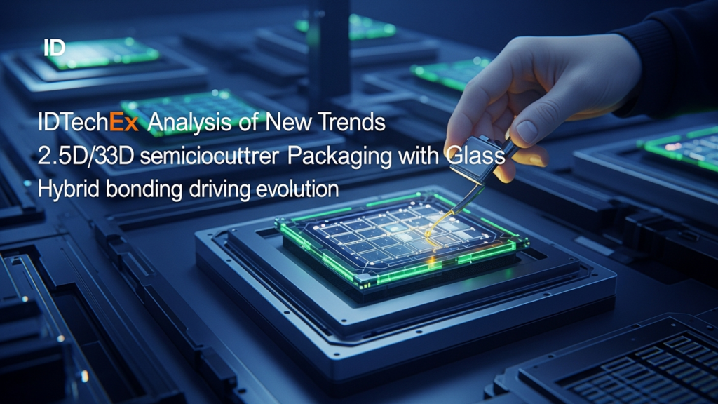
IDTechEx Analyzes New 2.5D/3D Semiconductor Packaging Trends: Glass Interposers and Hybrid Bonding Drive Evolution
IDTechEx UK Overview IDTechEx's analysis highlights glass interposers and hybrid bonding as critical emerging trends in semiconductor packaging. Glass interposers offer compatibility with panel-level packaging, promising cost-effective, ... -
AI Accelerates Shift to Panel Level Packaging (PLP) and Glass Core Substrates, Positioning Them as Pillars of Next-Gen Packaging
IEEE / Presentation USA Overview Driven by soaring demand from AI, automotive electronics, and consumer devices, advanced packaging is a critical enabler for enhanced performance, higher integration, and miniaturization in semiconductors...