Substrate– tag –
-

Mastering 3D-IC Verification Complexity: Multiphysics Analysis Key to Addressing Thermal, Mechanical Stress, and Reliability Challenges
Semiconductor Engineering USA Overview As the semiconductor industry transitions from 2D to 2.5D and 3D-IC configurations, verification complexity is escalating significantly. This article emphasizes the necessity of multiphysics analysi... -
Scanning Acoustic Microscopy (SAM) Enables High-Precision Non-Destructive Detection of Internal Defects in Semiconductor Packaging
Infinita Lab USA Overview Scanning Acoustic Microscopy (SAM) is highlighted as a critical non-destructive tool for high-precision evaluation of internal defects in semiconductors, electronic packaging, and material science. SAM excels at... -
Plasma Surface Engineering for Automotive Thermal Management Maximizes TIM Wettability to Minimize Thermal Resistance
KeyLink USA Overview Advanced plasma surface treatment has been introduced to significantly reduce contact thermal resistance in EV powertrain cooling systems. This technology elevates substrate surface energy to over 72 mN/m, achieving ... -
PatSnap Eureka Report: UV-Curable Adhesives Achieve Ultra-Fast Curing (2-3 seconds) for Accelerated Chip Embedding in Semiconductor Manufacturing
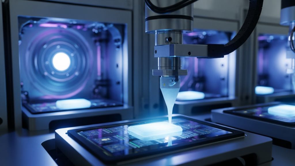
PatSnap Eureka Global Overview A PatSnap Eureka report reveals the semiconductor industry's increasing adoption of UV-curable adhesives for chip embedding due to their rapid curing capabilities and advantages in precision manufacturing. ... -
PatSnap Eureka Report: Optimizing Adhesive Coverage to Reduce Cell Delamination Risks in Advanced Packaging and Flexible Displays
PatSnap Eureka Global Overview A PatSnap Eureka report highlights the critical need for improved adhesive technologies and optimized coverage to prevent cell delamination in advanced semiconductor packaging and flexible display sectors. ... -
Samsung and Intel Pioneer Low-Warpage Solutions for Advanced Electronics Packaging, Boosting Reliability
PatSnap Eureka Global Overview Samsung and Intel are spearheading efforts to reduce warpage in electronics packaging components. Samsung leverages its I-Cube technology and optimized package stack designs to match thermal expansion chara... -
Siegwerk and Henkel Unveil Next-Gen Coatings to Drive Recyclable Packaging Forward
Packaging Europe ヨーロッパ Overview Siegwerk has introduced advanced heat-seal lacquers designed to enable fully recyclable flexible packaging by facilitating monomaterialization. Concurrently, Henkel Adhesive Technologies has significa... -
Plant Oil-Derived UV-Responsive Adhesives Offer Sustainable, Detachable Bonding for Enhanced Recycling
RSC Publishing Global Overview New research published in RSC Publishing details the synthesis and application of UV-responsive detachable polyurethane adhesives entirely derived from epoxidized plant oils, without synthetic photoinitiato... -
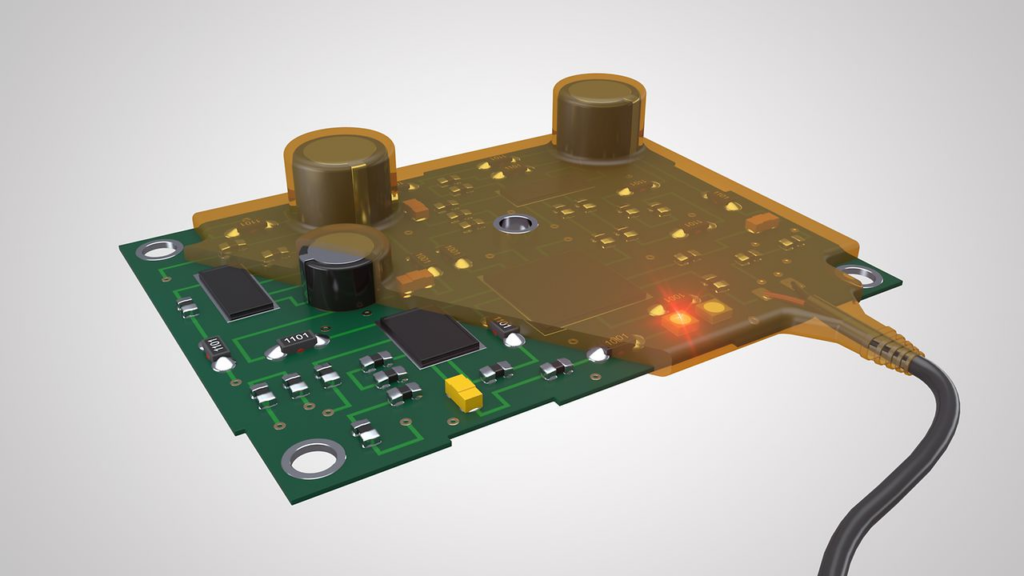
Henkel Unveils Ultra-Low Viscosity Technomelt PA 6370 for Rugged Electronics Protection and Accelerated Manufacturing
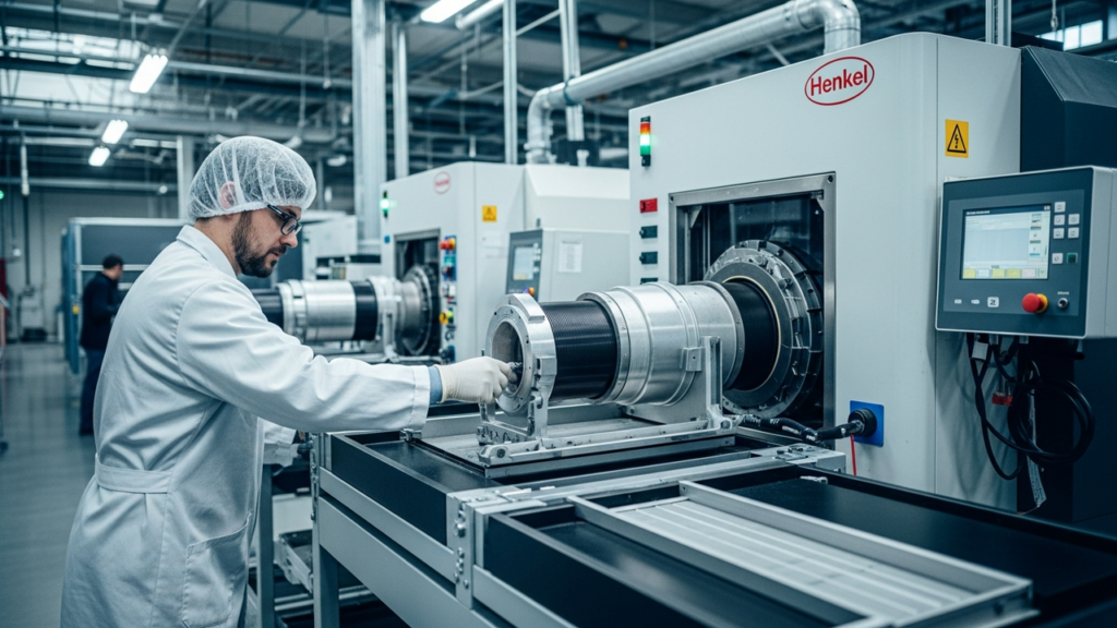
Henkel Germany Overview Henkel has launched Technomelt PA 6370, an ultra-low melt viscosity hot melt material designed for robust protection of challenging electronic device designs. This new polyamide-based material offers a high-speed,... -
Adhesive Type Critically Influences Delamination Risk and Recyclability in High-Stress Applications
PatSnap Eureka Global Overview Adhesive bonding technologies are evolving to join diverse materials with high reliability, though delamination remains a challenge, particularly in high-stress applications. While structural adhesives like...