Key Findings
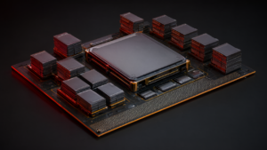
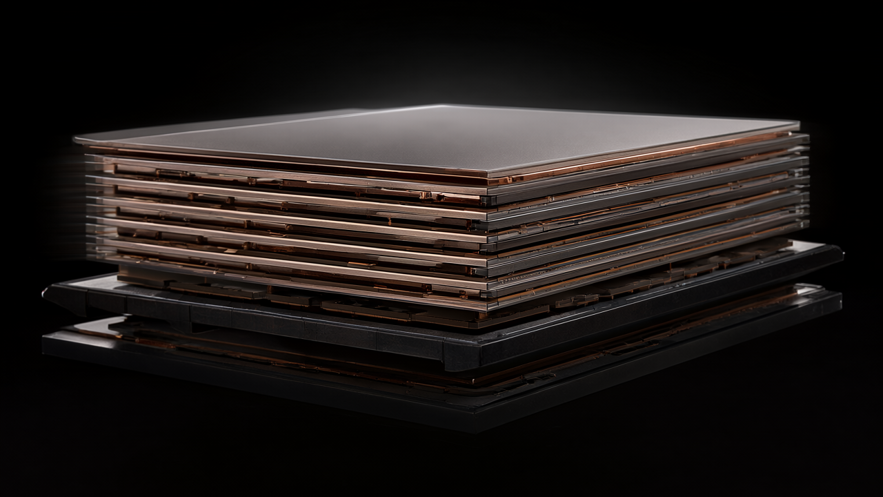
Samsung Electronics has introduced a groundbreaking thermal management solution for HBM4E, integrating a 4nm logic-based die with hybrid copper bonding (HCB) technology. This development allows Samsung to meet NVIDIA’s stringent requirement for a 775-micrometer HBM4 package height, demonstrating a more than 20% reduction in thermal resistance, a 30% improvement in heat dissipation, and a 40% enhancement in energy efficiency compared to HBM3E.
Technical / Clinical Details
The core of Samsung’s HBM4E solution lies in its dual technological advancements. Firstly, the use of a cutting-edge 4nm logic process for the base die, which manages data transfer between the HBM and AI accelerators. This not only curtails power consumption and heat generation from the base die but also enables a doubling of I/O terminals compared to HBM3E. Secondly, the implementation of Hybrid Copper Bonding (HCB) fundamentally improves interconnects. Unlike traditional micro-bump-based thermo-compression bonding (TCB), HCB directly bonds copper, achieving ultra-fine pitches below 10 micrometers and significantly boosting thermal conductivity. This results in reduced layer spacing, thinner stacks, and highly efficient heat dissipation, ultimately leading to a 20% plus reduction in overall thermal resistance. Further contributions to energy efficiency and thermal performance come from optimized low-voltage Through-Silicon Vias (TSVs) and an enhanced power delivery network.
Background & Context
As artificial intelligence continues its rapid expansion, HBM has become an indispensable component in high-performance computing, particularly for GPUs and AI accelerators. However, the increasing vertical stacking of HBM layers has exacerbated challenges related to package height and heat generation. Key customers like NVIDIA are pushing for thinner, cooler-running HBM modules, imposing package height standards below the JEDEC specification. Samsung’s latest innovation directly addresses these critical market demands, positioning the company to strengthen its competitive standing against rivals like TSMC and SK Hynix in the burgeoning HBM market.
Strategic Significance & Outlook
Samsung plans to begin customer qualification for its 16-layer HBM4E stacks in early 2027, a milestone that could significantly elevate its market presence in next-generation AI semiconductor supply. Beyond HCB, the company is also exploring alternative thermal mitigation techniques such as Heat Path Block (HPB) for HBM4E. This holistic approach to cooling, extending from the chip to the package and even system levels, indicates a strategic vision to push the boundaries of HBM technology. Such advancements are crucial for sustained improvements in computing performance and energy efficiency, vital for the continued growth of the AI era.
Get our weekly technology intelligence — free
Receive an infographic that lets you judge at a glance whether each field’s analysis report is worth reading.
Subscribe Free — Weekly Tech Intelligence
By subscribing, you’ll receive Troy-Technical’s weekly technology intelligence newsletter.
- Your email and selected fields are used only to deliver the newsletter.
- We never share your information with third parties.
- You can unsubscribe anytime via the link in each email.
See our Privacy Policy for details.
Takes about a minute · Unsubscribe anytime