Key Findings
Even as NVIDIA’s forthcoming Vera Rubin AI platform is expected to rely predominantly on 12-layer HBM4 memory chips, South Korean memory giants SK hynix and Samsung Electronics are pushing ahead with the development of more advanced 16-layer HBM4 technology. Samsung, in particular, has made strides with its hybrid copper bonding technique, which promises to support memory stacks beyond 16 layers and significantly reduce thermal resistance, positioning it ahead in this crucial innovation race.
Technical / Clinical Details
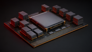
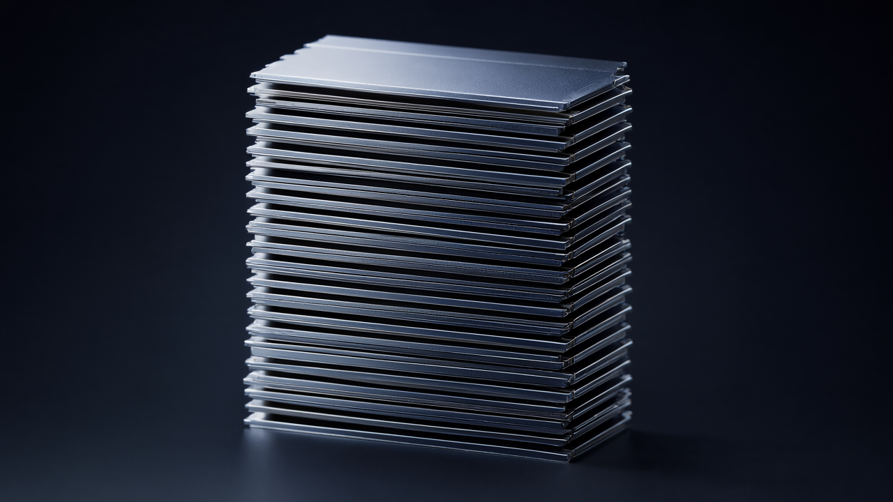
High Bandwidth Memory (HBM) involves stacking multiple DRAM dies vertically, connected via an interposer to a CPU or GPU, offering substantially higher bandwidth than traditional DRAM. The increasing demand for greater data throughput and capacity in AI applications necessitates higher stack counts. While NVIDIA’s Rubin platform targets 12 layers, SK hynix and Samsung are developing 16-layer HBM4 to meet future AI chip requirements. Samsung’s hybrid copper bonding technology, a key innovation, eliminates traditional chip bumps, directly bonding copper interconnects between silicon dies. This results in shorter connection distances, lower latency, enhanced performance, reduced signal distortion, and crucially, enables the physical feasibility of stacking 16 or more layers. SK hynix is optimizing HBM product integration with advanced packaging by collaborating closely with TSMC, emphasizing that HBM performance is not solely dependent on the memory itself but also on foundry packaging expertise.
Background & Context
The exponential growth in AI demand has fundamentally reshaped the DRAM industry, with HBM becoming a pivotal component. HBM manufacturing is considerably more complex than standard DRAM, yielding significantly fewer memory bits per wafer. High-performance AI chip production consumes over three times the wafer capacity compared to conventional DRAM. This disparity suggests that continued robust AI demand will likely sustain tight DRAM supply conditions across the industry. Major AI chip designers are therefore intensifying collaborations with memory manufacturers and foundries to secure stable supplies of high-performance HBM.
Strategic Significance & Outlook
The fierce competition between SK hynix and Samsung in 16-layer HBM4 development underscores the critical race for AI semiconductor performance leadership and market share. Innovative packaging technologies like hybrid copper bonding are indispensable for achieving higher HBM capacity, superior performance, and improved power efficiency, forming the bedrock of next-generation AI infrastructure. Bridging the gap between major customer roadmaps, such as NVIDIA’s, and memory manufacturers’ technological advancements will be crucial for market dynamics. As HBM’s proportion within the overall DRAM market increases, it is poised to further alter supply structures and significantly impact pricing strategies.
Source: https://m.koreaherald.com/article/10897751
Get our weekly technology intelligence — free
Receive an infographic that lets you judge at a glance whether each field’s analysis report is worth reading.
Subscribe Free — Weekly Tech Intelligence
By subscribing, you’ll receive Troy-Technical’s weekly technology intelligence newsletter.
- Your email and selected fields are used only to deliver the newsletter.
- We never share your information with third parties.
- You can unsubscribe anytime via the link in each email.
See our Privacy Policy for details.
Takes about a minute · Unsubscribe anytime