
Key Findings
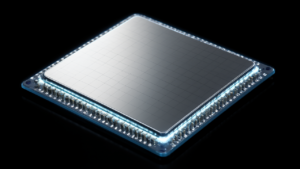
NVIDIA is developing next-generation CPO technology to bring optical engines closer to computing chips. At SEMICON West 2026, the company presented an optics-on-interposer (OOI) prototype and dense wavelength-division multiplexing (DWDM) technology. These research-stage developments are being evaluated for potential future products, though a commercialization timeline has not been announced.
Technical Details
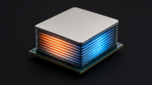
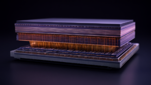
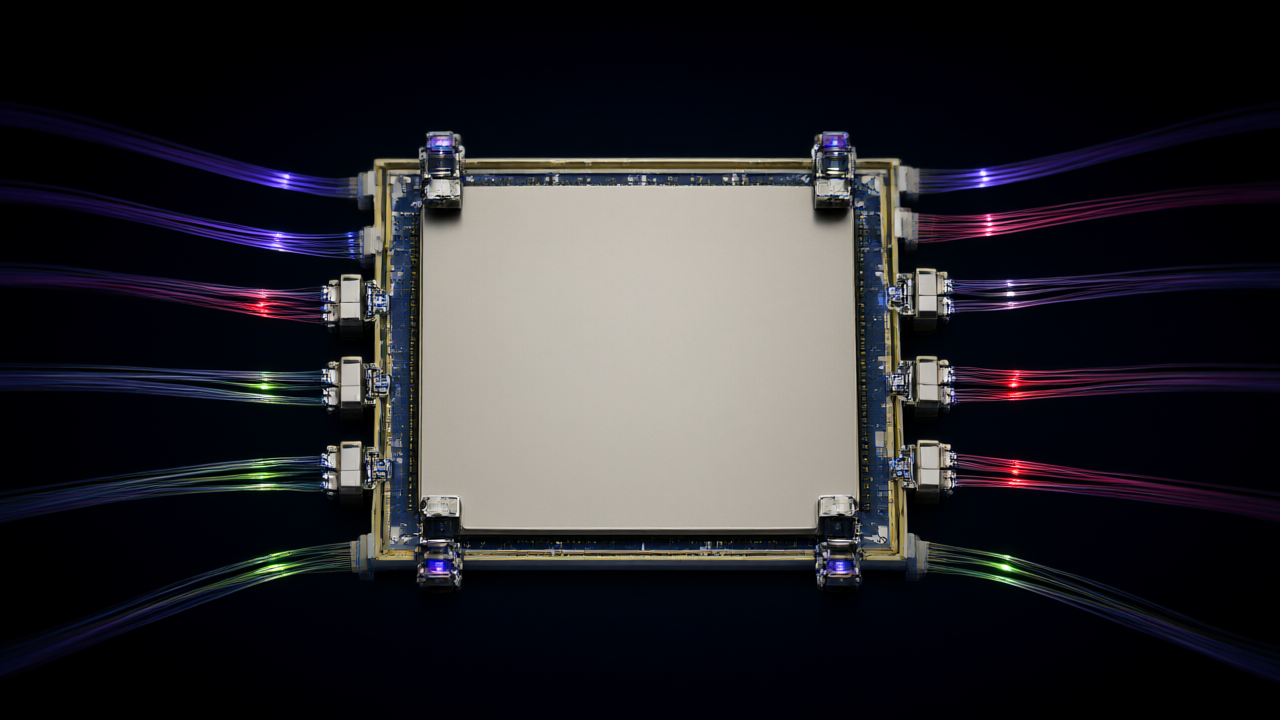
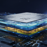
The OOI design relocates optical engines from the organic package substrate directly onto the silicon interposer. By eliminating the organic substrate from the electrical signal path, signals travel through shorter, fine-pitch interposer connections, which is intended to reduce power consumption and increase bandwidth density. Additionally, NVIDIA demonstrated DWDM technology that utilizes eight wavelengths operating at up to 32 Gb/s each, achieving an aggregate bandwidth of 256 Gb/s per single optical fiber.
Background and Context
NVIDIA has already commercialized CPO through its Spectrum-X Ethernet Photonics switches, which entered full production in May 2026. These switches integrate 200Gb/s SerDes with CPO for the Vera Rubin platform and have been adopted by Oracle Cloud Infrastructure, Lambda, and CoreWeave. This production is supported by a broad ecosystem: TSMC handles silicon photonics fabrication, SPIL manages chip-scale packaging and testing, TFC packages laser dies, and Foxconn integrates the switches into networking systems. Other partners include Coherent, Lumentum, Sumitomo Electric, Corning, Senko, Browave, and Fabrinet.
Significance and Outlook
Future AI system scaling will depend on balancing circuit design with thermal management and packaging challenges. NVIDIA plans to implement optical interconnects in its Kyber NVL1152 architecture, which connects eight racks into a single 1,152-GPU NVLink domain. This architecture will support the Feynman platform, which is expected to arrive in 2028. TrendForce notes that the CPO/NPO market is expected to exceed US$39 billion by 2030 as optical interconnects become critical for AI factory expansion.
Get our weekly technology intelligence — free
Receive an infographic that lets you judge at a glance whether each field’s analysis report is worth reading.
Subscribe Free — Weekly Tech Intelligence
By subscribing, you’ll receive Troy-Technical’s weekly technology intelligence newsletter.
- Your email and selected fields are used only to deliver the newsletter.
- We never share your information with third parties.
- You can unsubscribe anytime via the link in each email.
See our Privacy Policy for details.
Takes about a minute · Unsubscribe anytime