


Key Findings
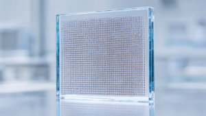
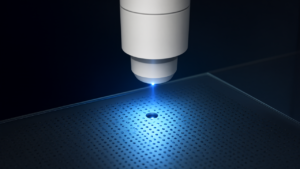
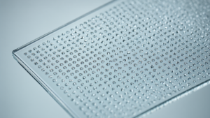
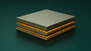
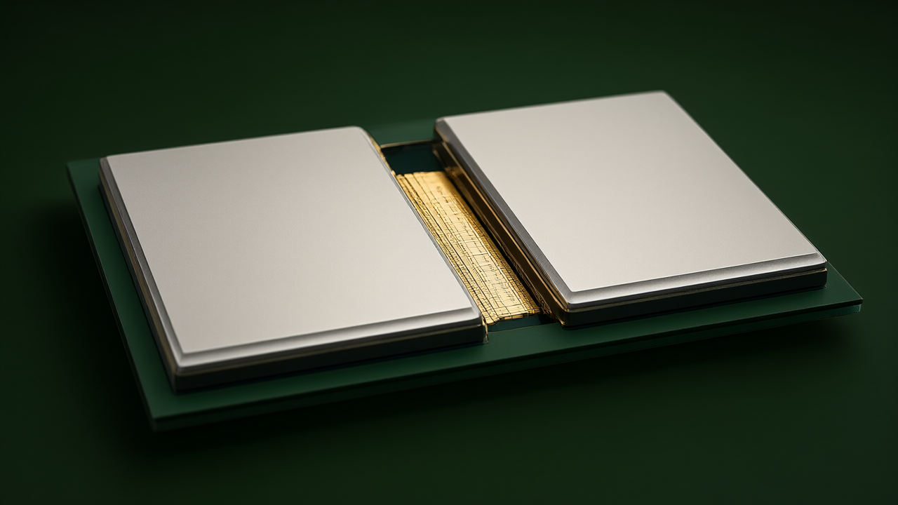
Intel reports that its Embedded Multi-die Interconnect Bridge (EMIB) technology achieves silicon wafer utilization of over 90%, significantly higher than the roughly 60% utilization seen in interposer-based designs. This efficiency is driven by the use of small, localized silicon bridges rather than a full-size interposer. Additionally, EMIB-T, which integrates through-silicon vias (TSVs) for power delivery, is gaining traction among major U.S. technology companies.
Technical Details and Roadmap
Intel’s roadmap for AI chip packages shows a trajectory of increasing size and complexity:
- 2026 Commercialization: Packages up to 120 × 120 mm, integrating 12 HBM stacks and more than 20 EMIB bridges.
- Current Development: Targets of at least 120 × 180 mm, featuring 16 or more HBM stacks and at least 38 bridges.
- Future Vision: Packages reaching 240 × 240 mm, integrating over 32 HBM stacks and more than 70 EMIB bridges.
Adoption and Supply Chain
Industry sources indicate that Google’s TPU v9 lineup may adopt EMIB-T for the HumuFish and TriggerFish models, while the WhaleFish model is expected to use TSMC’s CoWoS-L. Amazon is also reportedly planning to use EMIB-T for its custom AI chips. To support this ecosystem, Taiwanese foundry UMC manufactures EMIB silicon bridges using mature 12-inch wafer processes at its facilities in Taiwan and Singapore.
Competitive Landscape
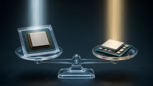
TSMC is pursuing similar scaling via CoWoS technology. In 2026, CoWoS-L is expected to support a 5.5X reticle-size package with four chiplets and 12 HBM stacks. By 2028, this is projected to scale to 14X, accommodating 20 chiplets and 20 HBM stacks. Meanwhile, reports indicate Intel’s EMIB substrate yields have hit 45%, with suppliers targeting 60% by 1Q27.
Get our weekly technology intelligence — free
Receive an infographic that lets you judge at a glance whether each field’s analysis report is worth reading.
Subscribe Free — Weekly Tech Intelligence
By subscribing, you’ll receive Troy-Technical’s weekly technology intelligence newsletter.
- Your email and selected fields are used only to deliver the newsletter.
- We never share your information with third parties.
- You can unsubscribe anytime via the link in each email.
See our Privacy Policy for details.
Takes about a minute · Unsubscribe anytime