

Key Findings
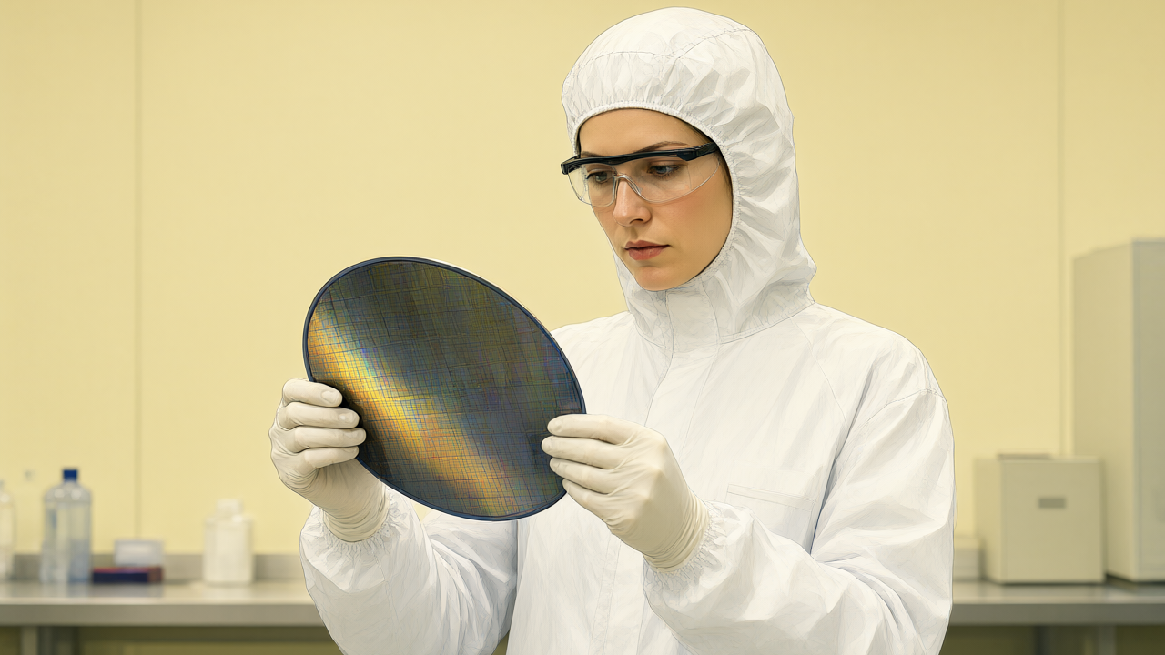
The National NanoFab Center (NNFC) has successfully implemented a test fabrication process for “silicon bridges,” marking the first time this capability has been available in a South Korean public nanofab. This infrastructure allows for the high-speed connection of multiple semiconductor chips, enabling domestic companies, universities, and research institutes to develop and verify advanced packaging technologies locally.
Technical Details
The NNFC Advanced Packaging Development Center research team developed the process based on 8-inch wafers. The technical specifications include:
- Fine Wiring: Copper wiring with a line width and spacing of approximately 1 micrometer (㎛), stacked in multiple layers to enable high-density electrical connections between chiplets.
- Vertical Connectivity: Integration of Through-Silicon Via (TSV) technology, which creates vertical conductive paths through the silicon to connect the top and bottom layers.
- Integrated Structure: The silicon bridge combines horizontal connectivity via fine wiring and vertical connectivity via TSV within a single structure.
- Additional Components: The process includes the fabrication of copper bumps for electrical contact and capacitors to stabilize power supply and reduce voltage fluctuations during high-speed operations.
- Standardization: The design incorporates concepts from the Universal Chiplet Interconnect Express (UCIe) international standard to ensure technical compatibility between chiplets from different manufacturers.
Background & Context
Silicon bridges act as data conduits between chiplets in a modular architecture. Rather than manufacturing a single large chip, the chiplet approach combines smaller, specialized chips (such as logic and memory) into one package. This increases design flexibility and is essential for AI semiconductors that require the rapid transfer of massive amounts of data.
Significance & Outlook
Previously, research into advanced packaging required significant costs to secure the necessary production equipment and process technology. By providing this public infrastructure, NNFC aims to support the entire lifecycle from initial R&D to prototype production and performance verification. This is expected to strengthen the competitiveness of the domestic semiconductor ecosystem, specifically for AI semiconductors and high-performance computing.
Source: https://www.joongangenews.com/news/articleView.html?idxno=561178
Get our weekly technology intelligence — free
Receive an infographic that lets you judge at a glance whether each field’s analysis report is worth reading.
Subscribe Free — Weekly Tech Intelligence
By subscribing, you’ll receive Troy-Technical’s weekly technology intelligence newsletter.
- Your email and selected fields are used only to deliver the newsletter.
- We never share your information with third parties.
- You can unsubscribe anytime via the link in each email.
See our Privacy Policy for details.
Takes about a minute · Unsubscribe anytime