Semiconductor Back-End– category –
-

Applied Materials Unveils New Systems to Propel DRAM & Advanced Packaging for AI Chips
StockTitan USA Overview Applied Materials has introduced a suite of new systems designed to dramatically enhance DRAM and advanced packaging processes, directly addressing the escalating performance demands of AI chips. These innovations... -
EU Chips Act Allocates €210M to Bolster 3D IC Packaging R&D for Strategic Semiconductor Autonomy
The Chosun Daily EU Overview The European Union has committed €210 million under its EU Chips Act to accelerate research and development in next-generation 3D IC packaging technologies. This significant investment aims to enhance Europe'... -
Semiconductor Back-End Weekly Report June 27, 2026
▼ ▼ ▼ If the infographic makes you want to read the full report, please click the download button below. ▼ ▼ ▼ 📄 Weekly Report June 27, 2026 (PDF) — Download Weekly Report June 27, 2026 (PDF) — DownloadDownload 🎙 Podcast June 27, 2026 (... -
SK hynix’s Early Strategic Investment in AI and HBM Drives Market Value Lead Over Samsung, Bolstering Production Capacity for NVIDIA Demand
Reuters South Korea Overview SK hynix's early and aggressive investment in HBM (High Bandwidth Memory) technology and significant capacity expansion, anticipating future NVIDIA demand, has allowed it to differentiate from Samsung Electro... -
HBM4E Set to Dominate High-Performance Memory Market by Late 2026-2027 with Up to 4.0 TB/s Single-Stack Bandwidth and 48GB+ Capacity, Accelerating AI Models
Ersa Electronics Global Overview HBM4E is projected to lead the high-performance memory market from late 2026 to 2027, offering a single-stack bandwidth of up to 3.6–4.0 TB/s and capacities exceeding 48GB, significantly boosting ultra-la... -
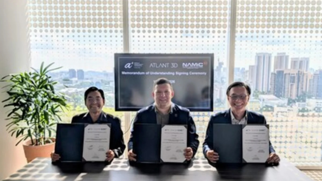
ATLANT 3D, A*STAR IMRE, and NAMIC Establish AI-Driven Materials Discovery Hub in Singapore to Accelerate Semiconductor and Advanced Packaging Innovation
Yahoo Finance Singapore Overview ATLANT 3D, A*STAR Institute of Materials Research and Engineering (IMRE), and National Additive Manufacturing Innovation Cluster (NAMIC) have signed an MOU to establish an Advanced Materials Development H... -
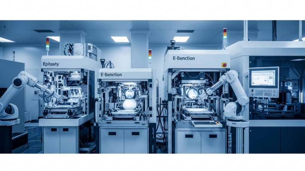
Applied Materials Unveils New Systems for DRAM and Advanced Packaging to Accelerate AI Chip Manufacturing, Featuring Epitaxy, CMP, and E-beam Inspection Technologies
Barchart.com USA Overview Applied Materials has introduced a suite of new chipmaking systems designed to accelerate the construction of advanced 3D chip architectures powering next-generation AI. This includes epitaxy systems optimizing ... -
Analog Technologies Delivers Specialized Advanced Packaging for Demanding Defense Systems Requiring Superior Thermal Management and Miniaturization
Analog Technologies USA Overview Analog Technologies offers specialized semiconductor packaging and interconnect capabilities for programs demanding advanced thermal management and miniaturized assemblies, particularly in defense systems... -
TSMC’s CoWoS Capacity Dramatically Expands, Eliminating Supply Constraint for NVIDIA B300 Servers and Cutting Lead Times to 8-16 Weeks
Contrary Research Taiwan Overview TSMC's CoWoS (Chip-on-Wafer-on-Substrate) packaging capacity has significantly expanded, effectively resolving a major GPU procurement constraint that had persisted for over six months in 2025. As a resu... -
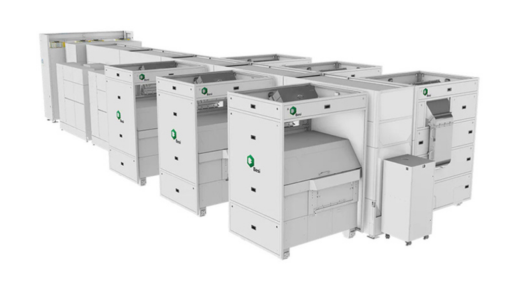
BE Semiconductor Industries (BESI) Raises Long-Term Revenue Target to €2.2 Billion and Operating Margin Target to 45% Amid Surging Hybrid Bonding Demand
Bits&Chips Netherlands Overview BE Semiconductor Industries (BESI) has significantly raised its long-term annual revenue target from €1.5-1.9 billion to €1.7-2.2 billion, while also increasing the lower end of its operating margin target...