HBM– tag –
-

Qnity Electronics Accelerates AI-Centric Advanced Packaging R&D with Expanded imec Collaboration
Converge Digest Belgium Overview Qnity Electronics has significantly expanded its strategic collaboration with imec, a world leader in nanoelectronics, to bolster long-term R&D in advanced semiconductor packaging crucial for AI and h... -
ECTC2026 Unveils Future of Semiconductor Packaging: Precision Adhesives and Low-Temperature Hybrid Bonding for HBM Integration
Tech I Japan Overview ECTC2026 highlighted critical R&D in advanced semiconductor packaging, showcasing innovations in chiplet integration, hybrid bonding, and opto-electronic convergence. Key presentations included Mitsui Chemicals ... -
ASMPT’s Advanced Packaging Business Achieves Record Sales in H1 2026, Driven by Surging AI Demand
ASMPT Singapore Overview ASMPT reported robust financial results for the first half of 2026, with its Advanced Packaging (AP) business achieving record sales, significantly propelled by escalating AI demand. Key contributors included The... -
TSMC Moves to Large-Format Glass Substrates with CoPoS to Address CoWoS Capacity for AI Chips, Targeting 2028-2029 Mass Production
36Kr, Semiconductor Industry Watch, AI Weekly Taiwan Overview TSMC has launched a pilot line for its CoPoS (Chip-on-Panel-on-Substrate) advanced packaging at Taiwan's VisEra, aiming to alleviate the critical CoWoS capacity bottleneck for... -
2.5D Packaging and HBM Integration Accelerate for AI Accelerators: TSMC CoWoS and Samsung I-CubeS Drive Towards 5.5x Reticle Sizes by 2026
Econ Market Research Global Overview The adoption of HBM-integrated 2.5D packaging for AI accelerators is rapidly expanding, with TSMC and Samsung spearheading the technological advancements. TSMC's CoWoS platform now supports silicon in... -
Intel Accelerates Next-Gen AI Semiconductor Development in U.S. Fabs with Foveros and Enhanced EMIB-T Packaging
Intel USA Overview Intel is aggressively advancing next-generation AI semiconductor development in its U.S. fabs by leveraging cutting-edge advanced packaging technologies such as Foveros stacking, EMIB silicon bridges, and particularly ... -
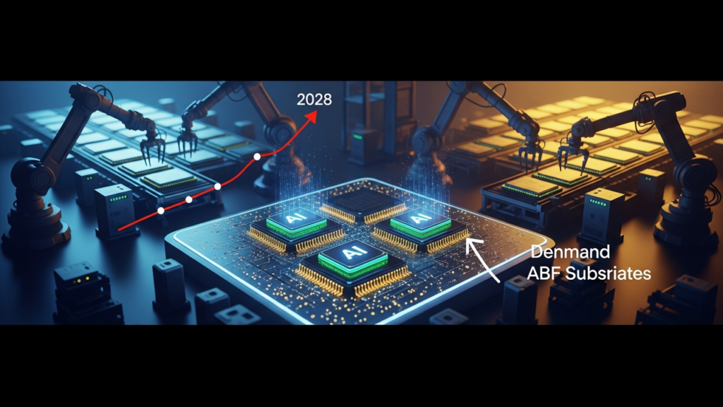
AI Chip HBM Integration to Drive 29% ABF Substrate Shortage by 2028; $19.1B Expansion Unlikely to Offer Short-Term Relief
Unknown Taiwan Overview The rapid integration of High Bandwidth Memory (HBM) into AI chips is set to drive a 39% Compound Annual Growth Rate (CAGR) in ABF substrate demand between 2025 and 2028. This surge is projected to create a supply... -
Intel’s EMIB Dominates AI Packaging with Google Adoption, Prompting TSMC to Develop Similar Tech Amidst CoWoS Constraints
Benzinga USA Overview Intel's EMIB technology is establishing a significant competitive advantage in advanced chip packaging for AI workloads, exemplified by Google's adoption of EMIB-T in its 9th-generation TPUs. Facing CoWoS capacity f... -
Malaysia Invests US$45 Million to Propel Advanced Chip Packaging, Targeting HBM4 Domestic Proof-of-Concept
Asia News Network Malaysia Overview Malaysia announced a 185 million ringgit (approx. US$45 million) investment into semiconductor projects to boost its advanced chip packaging capabilities for AI, data centers, and high-performance comp... -
Besi Achieves Record €292.9M Orders in Q2 2026, Driven by AI Demand and 128.8% Growth in Hybrid Bonding Technology
ET Electronics News Netherlands Overview BE Semiconductor Industries (Besi) reported record Q2 2026 orders of €292.9 million, a 128.8% increase year-over-year, primarily fueled by robust AI-related demand and the surging adoption of its ...