HBM– tag –
-

Applied Materials Launches New HBM & 3D Packaging Systems, Acquires ASMPT NEXX to Scale AI Compute
Exoswan Insights USA Overview Applied Materials has introduced new CMP, ECD, deposition, and e-beam systems for HBM and 3D packaging, alongside acquiring ASMPT's NEXX business, to capitalize on the escalating demand for AI computing. The... -
AI Boom Spurs China’s Top OSATs to Pour Billions into Advanced Packaging
Digital Today China Overview China's three leading OSAT firms—JCET, Tongfu Microelectronics, and Huatian Technology—have reported significant profit surges in H1 2026, largely due to escalating AI semiconductor demand. In response, these... -
Powertech Aims for Early 2027 Launch of World’s First AI Server Panel-Level Packaging Mass Production
Tonarism Taiwan Overview Powertech Technology, a leading Taiwanese OSAT, has unveiled plans to commence mass production of panel-level packaging (PLP) for AI semiconductors and server CPUs by early 2027. This initiative establishes the w... -
Taiwan’s OSATs Boost AI Capacity with $14.4B Capex; ASE Deepens TSMC CoWoS Collaboration to Meet Soaring Demand
Domino Theory Taiwan Overview Five leading Taiwanese chip packaging and test companies plan a record $14.4 billion (NT$460 billion) in capital expenditures this year to meet surging AI chip demand, matching TSMC's own advanced packaging ... -
SK hynix’s MR-MUF and Samsung’s TC-NCF Revolutionize Thermal Management in AI Semiconductor HBM: Driving Advanced Packaging Evolution
USD Analytics Global Overview The evolution of AI is driving significant changes in semiconductor packaging and High Bandwidth Memory (HBM) technologies, with SK hynix's Advanced MR-MUF and Samsung's TC-NCF technologies solving critical ... -
AI Advancements Drive New Semiconductor Packaging Paradigm: Panel-Based Technologies Surpass Traditional Silicon Interposer Limits
Facebook (reposting an industry trend) USA Overview The rapid evolution of AI is pushing semiconductor packaging beyond the practical limits of traditional silicon interposers, driving a new paradigm. Panel-based packaging is emerging as... -
Glass Substrates in Advanced Packaging Accelerate from Prototype to Mass Production, Emerging as Key Technology for HBM and Chiplet Integration
Solid State Technology USA Overview Advanced packaging technology utilizing glass substrates is rapidly transitioning from R&D to mass production within the semiconductor industry. Glass substrates, superior to conventional organic s... -
AT&S Ramps Up HPC Substrate Capacity to Meet Surging Data Center and AI Demand
Business Journal Austria Overview Austrian-based AT&S, a leading package substrate manufacturer, is significantly accelerating its IC substrate capacity expansion, primarily targeting high-performance computing (HPC) applications. Th... -
imec Pioneers Glass Substrates for Next-Gen 3D Packaging, Accelerating AI/HPC Commercialization
EETimes Belgium Overview imec, the renowned Belgian microelectronics research institute, has announced a significant breakthrough in 3D stacked packaging, leveraging glass substrates as interposers. This innovation is pivotal for next-ge... -
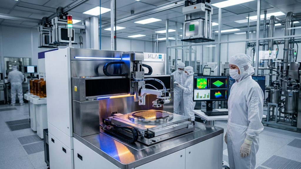
KLA Unveils AI-Powered High-Speed, High-Precision Defect Inspection Solution to Boost Yield in Advanced Packages like CoWoS
SEMI Global USA Overview KLA has introduced a new AI-powered inspection system for high-speed, high-precision defect detection in high-density RDLs and 3D stacked structures. This solution supports yield management in advanced packaging ...