Intel– tag –
-

Advanced Packaging: Glass Core Substrates Emerge as Next-Gen Frontier; Intel Commits Over $1 Billion to R&D for High-Volume Production by 2030
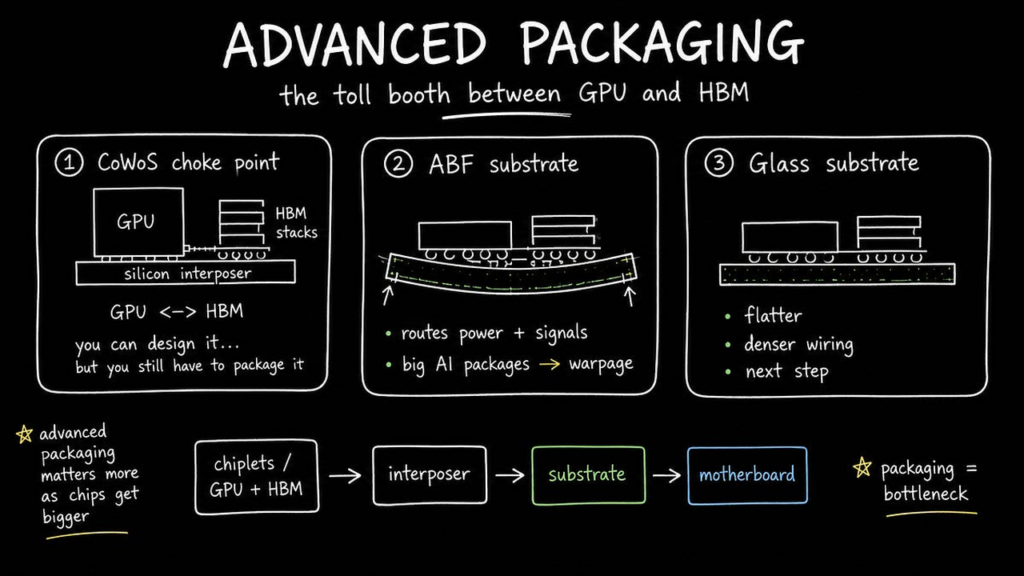
Infra Startups USA Overview Advanced packaging is a critical bottleneck in the AI boom, with TSMC's CoWoS capacity dictating the pace of global AI infrastructure build-out. Shipments of CoWoS wafers are projected to reach approximately 4... -
TechInsights Identifies Silicon Photonics as Backbone for HPC and AI Data Centers, Highlighting New Industry Opportunities
TechInsights Blog Canada Overview TechInsights' analysis highlights silicon photonics as an indispensable backbone rapidly emerging for High-Performance Computing (HPC) and AI data centers. This technology overcomes the limitations of tr... -
ECTC 2026: Intel Foundry and Amkor Announce Advanced Packaging Technologies for AI/HPC and U.S. Manufacturing Capacity Expansion
Intel Newsroom, Amkor Technology Blog, Semiconductor Engineering USA Overview The 2026 IEEE Electronic Components and Technology Conference (ECTC) showcased advanced packaging technologies redefining scalability limits for AI and high-pe... -
TSMC’s COUPE Platform for Co-Packaged Optics Targets 2026 Mass Production, Integrating Micro LEDs for AI Cluster Performance Boost
The Storm Media Taiwan Overview TSMC has announced the 2026 mass production launch of "COUPE" (Compact Universal Photonic Engine), an innovative platform for co-packaged optics (CPO) interconnects. Utilizing SoIC bonding to stack photoni... -
Intel and Tesla Partner on AI6 Data Centers, Tapping Advanced Packaging for Production at Austin’s ‘Terafab’
Jamie's Substack USA Overview Tesla has announced a strategic partnership with Intel Foundry Services to scale its AI6 chip-powered data center clusters, extensively utilizing Intel's advanced packaging technologies. The collaboration wi... -
Advanced Packaging’s Evolution: 2.5D/3D Integration, Chiplets, and Hybrid Bonding Propel AI and HPC
Springer Professional Germany Overview Semiconductor packaging technology has dramatically evolved from 2D to 2.5D and 3D IC integration, a transformation accelerated by the explosive demand from AI and High-Performance Computing (HPC). ... -
Glass Substrates: The Next Frontier in AI Packaging and the Race to Mass Production
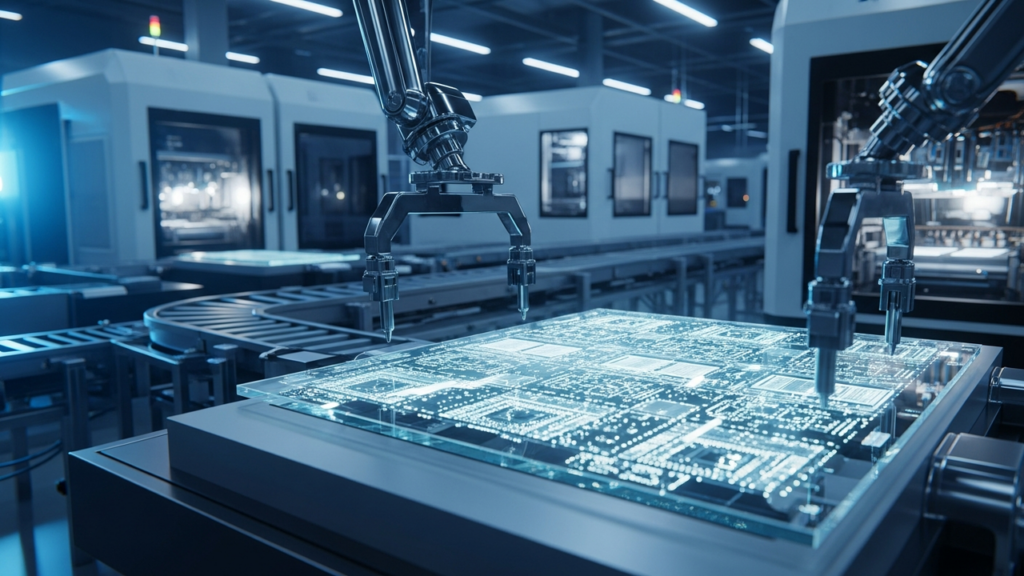
The Economy South Korea Overview Glass substrates are rapidly emerging as a transformative technology in advanced AI chip packaging, poised to replace conventional organic substrates and silicon interposers by offering superior dimension... -
Amkor Bolsters U.S. Semiconductor Ecosystem with Over $7 Billion Investment in Arizona Advanced Packaging Facility
Amkor USA Overview Amkor Technology is dramatically escalating its commitment to a new advanced packaging and test facility in Peoria, Arizona, increasing its investment from an initial $2 billion to over $7 billion. This strategic expan... -
Silicon Box Secures $77.5M to Scale Advanced Packaging and Chiplet Integration
DealStreetAsia Singapore Overview Singapore-based semiconductor packaging and chiplet integration startup, Silicon Box, has secured S$100 million (approximately US$77.5 million) in debt financing from a global consortium of institutional... -
Samsung to Establish Gwangju Advanced Packaging Facility, Eyes Full HBM Hybrid Bonding Transition by 2029
TrendForce South Korea Overview Samsung Electronics is reportedly considering a new advanced semiconductor packaging plant in Gwangju, South Korea, with investment plans potentially announced by June 2026. This strategic facility will fo...