

Key Findings: API Showcases High-Performance Bonding Platforms at SEMICON Taiwan 2026, Receiving Strong International Acclaim
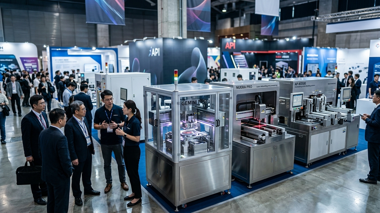
Following the conclusion of SEMICON Taiwan 2026, API (Advanced Packaging Intelligence) announced a significant success in showcasing its advanced packaging solutions designed to support next-generation semiconductor manufacturing. The company’s featured in-line bonding platforms—GEMINI PRO, NUERA PRO, and AP-M3500—address critical challenges in advanced packaging, including heterogeneous bonding, package warpage control, and AMHS (Automated Material Handling System) fab integration. These innovations attracted substantial interest from international customers.
Technical Details: Addressing Major Packaging Bottlenecks
- GEMINI PRO Platform: This platform delivers high-precision die bonding and high-efficiency throughput, meeting the demands of complex heterogeneous integration. It enables the high-density integration of chips with different functionalities into a single package.
- NUERA PRO Platform: Features technology designed to effectively control warpage, a significant issue particularly with large substrates and thinned packages. Warpage control is crucial as it directly impacts bonding accuracy and final product yield.
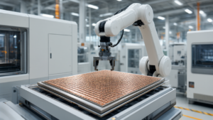
- AP-M3500 In-line Bonding Platform: Offers high-speed and high-precision bonding processes seamlessly integrated with automated material handling systems (AMHS) in semiconductor fabrication lines. This significantly enhances overall fab production efficiency and data management.
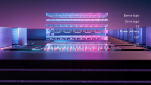
- Key Challenges Addressed: The exhibition highlighted how these products provide effective solutions for technical bottlenecks in next-generation packaging, such as fine-pitch interconnects, thermal management, and power delivery.
Background & Industry Context: Indispensability of Advanced Packaging in the AI Era
The increasing demand for high-performance computing in areas like AI, HPC, and 5G communications presents new challenges for semiconductor chip design and manufacturing. Traditional single-chip performance scaling is reaching its limits, making advanced technologies such as heterogeneous integration (combining multiple chiplets) and 2.5D/3D packaging indispensable. The realization of these technologies critically depends on high-precision bonding equipment and robust quality/productivity management throughout the manufacturing process, elevating the role of equipment suppliers like API.
Strategic Significance & Outlook: Contributing to Semiconductor Industry Efficiency and Performance
API’s advanced bonding solutions directly contribute to the efficiency of semiconductor manufacturing processes and the next-generation chips performance improvement. The strong international customer interest demonstrates that these technologies are addressing urgent market needs, suggesting potential for API to expand its market share and contribute to industry standardization. As the AI era progresses, the demand for more complex and sophisticated packaging solutions is expected to grow, positioning API as a key player in this evolving landscape.
Source: https://www.sgapi.com/news/33
Get our weekly technology intelligence — free
Receive an infographic that lets you judge at a glance whether each field’s analysis report is worth reading.
Subscribe Free — Weekly Tech Intelligence
By subscribing, you’ll receive Troy-Technical’s weekly technology intelligence newsletter.
- Your email and selected fields are used only to deliver the newsletter.
- We never share your information with third parties.
- You can unsubscribe anytime via the link in each email.
See our Privacy Policy for details.
Takes about a minute · Unsubscribe anytime