Chiplet– tag –
-

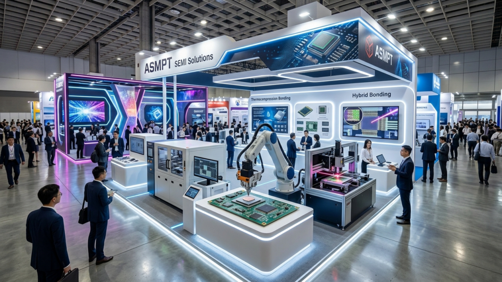
ASMPT to Showcase Advanced Thermocompression and Hybrid Bonding Innovations for HPC and AI at SEMICON Taiwan 2026
ASMPT SEMI Solutions Taiwan Overview Global technology leader ASMPT announced it will showcase its advanced packaging portfolio at SEMICON Taiwan 2026, supporting HPC, AI accelerators, silicon photonics, and Co-Packaged Optics (CPO) appl... -
Rapidus Targets 600mm Panel-Level Packaging and 8-Reticle Interposers by 2030 for Advanced AI/HPC Systems
TrendForce Japan Overview Rapidus announced an accelerated advanced packaging roadmap aiming for 600mm panel-level packaging and 8-reticle interposers by 2030. The company has fully activated its Rapidus Chiplet Solutions (RCS) pilot lin... -
Semiconductor Foundries Evolve Role, Driving Industrialization of Silicon Photonics and Advanced Heterogeneous Integration
Design And Reuse USA Overview Semiconductor foundries are shifting their role from pure transistor manufacturing to providing advanced packaging and heterogeneous integration solutions. This evolution is crucial for the burgeoning chiple... -
Rapidus Targets 8-Reticle Interposers on 600mm Advanced Packaging Panels by 2030, Accelerating Heterogeneous Integration for AI/HPC
Design And Reuse Japan Overview Japanese foundry Rapidus has unveiled an ambitious roadmap to achieve 8-reticle interposers on 600mm advanced packaging panels by 2030. This development is crucial for integrating complex chiplets, includi... -
Hot Chips 2026: South Korea’s BOS Semiconductors Unveils ‘Eagle-N’ AI Accelerator with up to 2,000 TOPS for Physical & Automotive AI
The Elec Inc. South Korea Overview At Hot Chips 2026, South Korean BOS Semiconductors introduced 'Eagle-N,' an AI accelerator specifically designed for physical and automotive AI applications. This innovative chip boasts a data-efficient... -
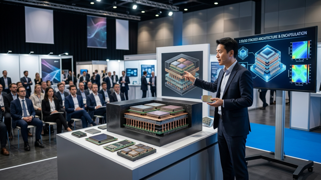
Sumitomo Bakelite Unveils Novel Low-Stress Epoxy Compound for Next-Gen 2.5D/3D Packaging
SEMI Europe Conference News Japan Overview Sumitomo Bakelite has announced a groundbreaking epoxy molding compound (EMC) at SEMI Europe, specifically engineered for the intricate demands of 2.5D and 3D advanced packaging solutions. This ... -
Henkel Unveils Advanced EMC to Tackle Warpage and Thermal Challenges in Next-Gen AI Processors
Henkel Corporate Press Release Germany Overview Henkel has introduced a novel epoxy molding compound (EMC) engineered specifically for high-performance AI and HPC processors. This innovative material significantly reduces thermal-induced... -
Lens Technology Enters Advanced Chip Packaging with Self-Developed Through-Glass Vias (TGV) Substrates and Dedicated 30,000sqm Factory
Chinadaily.com.cn China Overview Chinese smartphone glass screen manufacturer Lens Technology has announced its entry into the advanced chip packaging market, driven by AI chips pushing traditional material limits. The company showcased ... -
Morgan Stanley Taps Samsung Electro-Mechanics as Top Korean Tech Pick Amid Surging AI Chip Substrate Demand
Evrim Ağacı Turkey Overview Morgan Stanley has elevated Samsung Electro-Mechanics to its premier Korean tech stock, citing the escalating technical demands of AI chip designs on advanced substrates. As AI processors become larger, multi-... -
Japan’s Shinko Electric Develops 22-Layer Glass Substrates for AI Chips, Resolving Internal Cracking and Delamination Issues
TrendForce Japan Overview As AI chips demand larger packages, intensifying competition in glass substrates, Japan's Shinko Electric Industries has successfully developed 22-layer glass substrates with 11 copper wiring layers on each side...