Chiplet– tag –
-

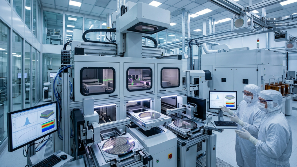
KLA’s Advanced Packaging Business Set for $1.1 Billion Revenue, 70%+ Growth Driven by AI Demand and Yield Bottleneck Resolution
Quartz USA Overview KLA is significantly benefiting from accelerating demand for advanced packaging inspection, metrology, and process control tools due to the increasing complexity of AI/HPC chips and hybrid bonding advancements. Its ad... -
Intel’s EMIB-T Advanced Packaging Projected for Significant Contribution by 2029 as CoWoS Constraints Drive Google’s Interest
TrendForce Taiwan Overview Intel's EMIB (Embedded Multi-die Interconnect Bridge) technology, particularly EMIB-T, is attracting strong interest from major tech firms like Google amid persistent TSMC CoWoS supply constraints. Intel projec... -
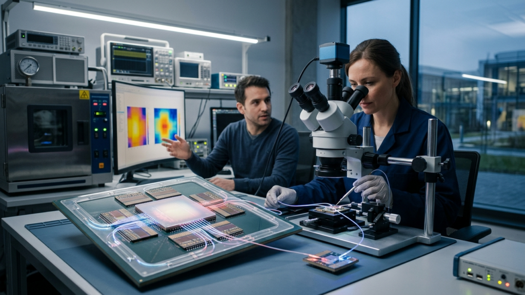
Semiconductor Engineering Analyzes: Photonics Forces Chiplet Rethink, Multi-Physics Co-Design to Solve Thermal, Stress, Alignment Challenges
Semiconductor Engineering USA Overview Semiconductor Engineering reports that the integration of photonics is fundamentally forcing a reevaluation of chiplet design. Due to the bidirectional interaction of thermal, mechanical, electromag... -
Marvell Expands Photonic Fabric with Google TPU Ecosystem Partnership, 8 Tbps Optical I/O Chiplet Demo, and Celestial AI Acquisition
FUNDA | Substack USA Overview Google and Marvell announced a strategic partnership for custom silicon programs connecting to the TPU ecosystem, leading Marvell to significantly increase its FY27 revenue outlook for scale-up optics. Ayar ... -
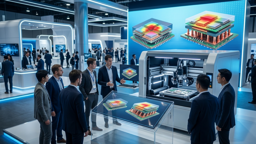
Epsilon Unveils Advanced Semiconductor Packaging Materials at ASPS 2026 for AI Data Centers: Die Attach Copper Paste Improves Thermal Dissipation and Reduces Cost
The Elec Inc. South Korea Overview Epsilon showcased advanced packaging material solutions at the 2026 Advanced Semiconductor Packaging & Chiplet Show (ASPS 2026), targeting advancements in AI data centers. Exhibited materials includ... -
Koh Young to Unveil Advanced Packaging Measurement Technologies for AI, Chiplet, and Thermal Management at Electronics Packaging Symposium 2026
I-Connect007 South Korea Overview Koh Young Technology will participate in the 37th Annual Electronics Packaging Symposium (EPS 2026) to address measurement challenges in advanced packaging for AI, chiplet architectures, heterogeneous in... -
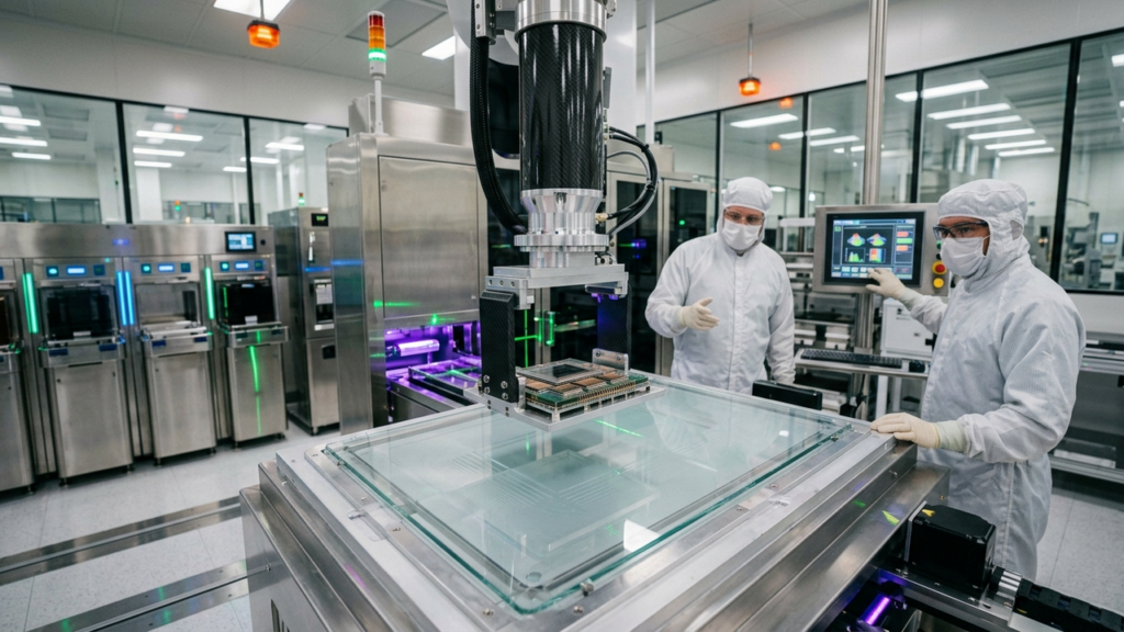
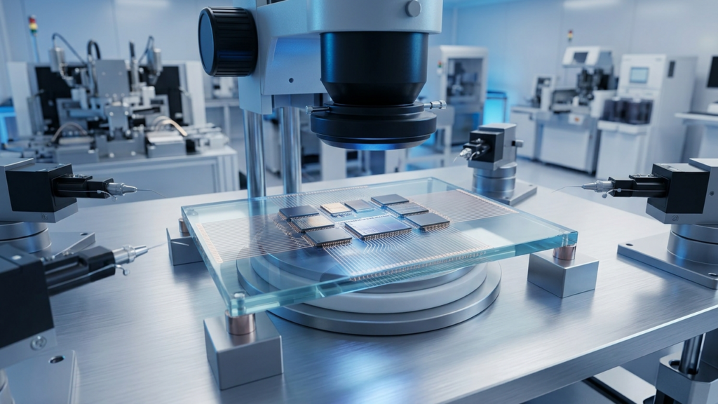
Glass Substrates in Advanced Packaging Accelerate from Prototype to Mass Production, Emerging as Key Technology for HBM and Chiplet Integration
Solid State Technology USA Overview Advanced packaging technology utilizing glass substrates is rapidly transitioning from R&D to mass production within the semiconductor industry. Glass substrates, superior to conventional organic s... -
Infineon Strengthens Advanced Packaging Collaboration in Europe under EU Chips Act, Building Chiplet and Heterogeneous Integration Supply Chain
Reuters Germany Overview Infineon announced strengthened partnerships for advanced packaging technology development within Europe, leveraging the EU Chips Act. This strategy aims to build an indigenous supply chain for chiplet technology... -
imec Pioneers Glass Substrates for Next-Gen 3D Packaging, Accelerating AI/HPC Commercialization
EETimes Belgium Overview imec, the renowned Belgian microelectronics research institute, has announced a significant breakthrough in 3D stacked packaging, leveraging glass substrates as interposers. This innovation is pivotal for next-ge... -
Applied Materials Unveils New Hybrid Bonding Platform for High-Volume 3D Stacked Chip Manufacturing, Enabling Ultra-Fine Pitch Integration
Business Wire USA Overview Applied Materials has launched a new hybrid bonding platform designed for high-volume manufacturing of next-generation 3D stacked chips. This innovative system achieves high-precision alignment and high through...