Glass Substrate– tag –
-

TSMC Accelerates CoPoS Packaging Development, Standardizing 310x310mm Panel Format; Introduces Glass Core Substrate for CoWoS Towards Late 2028 Mass Production
TrendForce Taiwan Overview TSMC is accelerating the development of its CoPoS (Chip-on-Panel-on-Substrate) packaging architecture, standardizing a 310x310mm panel format, with pilot production targeted for 2027 and mass production in late... -
Semiconductor Engineering June 2026 Report Highlights On-Chip Photonics, Hybrid Bonding, and GaN for AI/HPC
Semiconductor Engineering USA Overview Semiconductor Engineering's June 2026 issue features on-chip photonics for AI systems, enhanced connectivity via hybrid bonding, new GaN power device designs, and managing manufacturing variations a... -
TSMC’s CoWoS Shortage Eases, But Bottleneck Shifts to ‘Hyper-Scale Packaging’ as Google Reportedly Engages Samsung for TPU Production
Zhitong Finance APP Hong Kong Overview Reports suggest Google is in discussions with Samsung Electronics regarding the production of specific hardware components for its AI training and inference Tensor Processing Units (TPUs), highlight... -
Glass Core Substrates Emerge as Next-Gen AI/HPC Packaging Technology, Face Commercialization Hurdles in Brittleness and TGV Formation
Pandaily China Overview Glass core substrates are garnering significant attention in the semiconductor packaging industry, driven by escalating performance demands in AI chips, HPC, and advanced processor packaging. They offer superior d... -
TSMC Strengthens Glass Substrate Supply Chain for CoWoS, Achieving 16% Warpage Reduction for High-Performance AI GPUs
Wccftech USA Overview TSMC is expanding its glass substrate supply chain for advanced CoWoS packaging, collaborating with Innolux and Ibiden. Glass substrates demonstrate a 16% reduction in package warpage, along with improved thermal ex... -
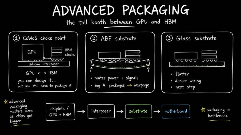
ABF Substrates Become AI Accelerator Bottleneck, Nvidia’s H100 Requires 12+ Layers; Glass Substrates Emerge as Next-Gen Solution, Commercialization Years Away
Data Gravity USA Overview Ajinomoto Build-up Film (ABF) substrates are a critical component and growing bottleneck in AI accelerators, HBM, and chiplet-based designs. Nvidia's H100 GPU demands over 12 layers of ABF, with the Blackwell B2... -
Advanced Packaging: Glass Core Substrates Emerge as Next-Gen Frontier; Intel Commits Over $1 Billion to R&D for High-Volume Production by 2030
Infra Startups USA Overview Advanced packaging is a critical bottleneck in the AI boom, with TSMC's CoWoS capacity dictating the pace of global AI infrastructure build-out. Shipments of CoWoS wafers are projected to reach approximately 4... -
Glass Substrates: The Next Frontier in AI Packaging and the Race to Mass Production
The Economy South Korea Overview Glass substrates are rapidly emerging as a transformative technology in advanced AI chip packaging, poised to replace conventional organic substrates and silicon interposers by offering superior dimension... -
TSMC to Boost CoWoS Capacity Tenfold to 130K Wafers/Month by Late 2026, Accelerates Glass-Substrate CoPoS for AI Chips
Tom's Hardware USA Overview TSMC is aggressively expanding its advanced packaging capacity, projecting a tenfold increase in CoWoS production to over 130,000 wafers per month by the end of 2026 to meet surging AI demand. Despite this, de... -
IEEE ECTC 2026 Program Reveals Latest Research in Advanced Packaging, Including 3D Integration, Hybrid Bonding, and New Substrate Materials
IEEE Electronic Components and Technology Conference (ECTC) USA Overview The program for the 76th IEEE Electronic Components and Technology Conference (ECTC) unveiled a wide array of cutting-edge research in advanced packaging, focusing ...