Glass Substrate– tag –
-

Glass Substrates in Advanced Packaging Accelerate from Prototype to Mass Production, Emerging as Key Technology for HBM and Chiplet Integration
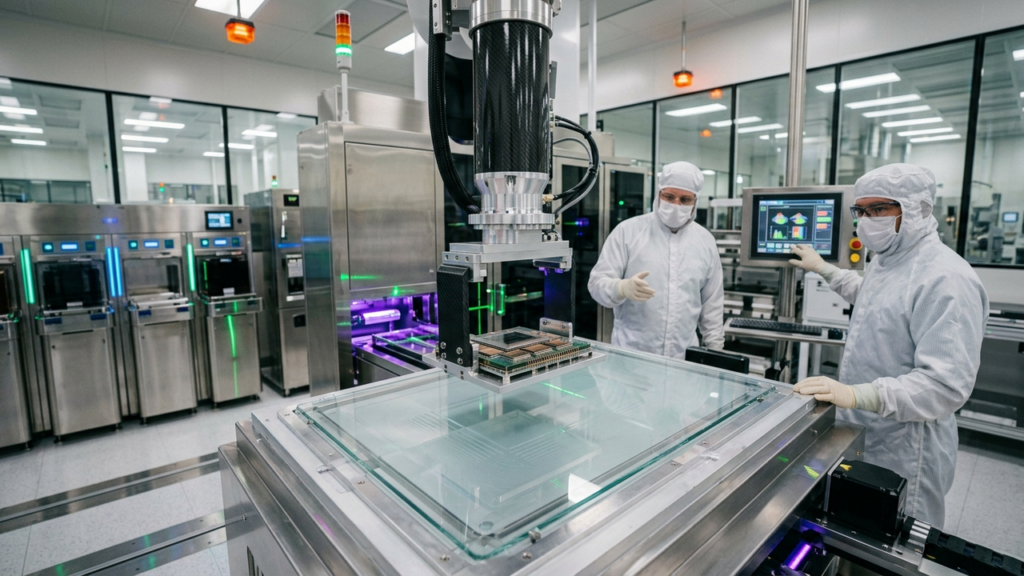
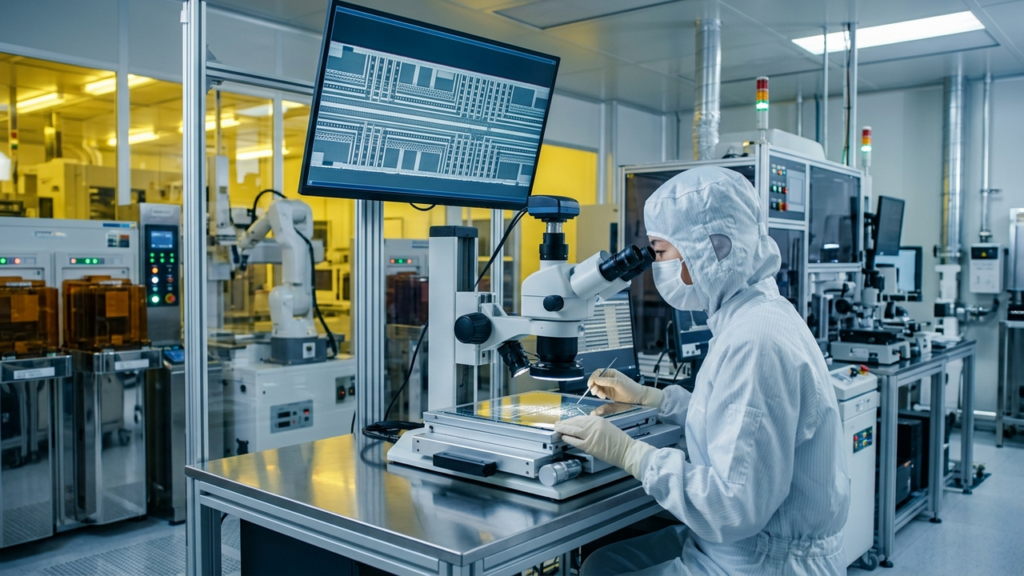
Solid State Technology USA Overview Advanced packaging technology utilizing glass substrates is rapidly transitioning from R&D to mass production within the semiconductor industry. Glass substrates, superior to conventional organic s... -
imec Pioneers Glass Substrates for Next-Gen 3D Packaging, Accelerating AI/HPC Commercialization
EETimes Belgium Overview imec, the renowned Belgian microelectronics research institute, has announced a significant breakthrough in 3D stacked packaging, leveraging glass substrates as interposers. This innovation is pivotal for next-ge... -
Lens Technology Enters Advanced Chip Packaging with Self-Developed Through-Glass Vias (TGV) Substrates and Dedicated 30,000sqm Factory
Chinadaily.com.cn China Overview Chinese smartphone glass screen manufacturer Lens Technology has announced its entry into the advanced chip packaging market, driven by AI chips pushing traditional material limits. The company showcased ... -
Japan’s Shinko Electric Develops 22-Layer Glass Substrates for AI Chips, Resolving Internal Cracking and Delamination Issues
TrendForce Japan Overview As AI chips demand larger packages, intensifying competition in glass substrates, Japan's Shinko Electric Industries has successfully developed 22-layer glass substrates with 11 copper wiring layers on each side... -
Samsung Electro-Mechanics Fast-Tracks Glass Substrates for AI Chip Packaging, Challenging Japanese Rivals for 2028 Mass Production
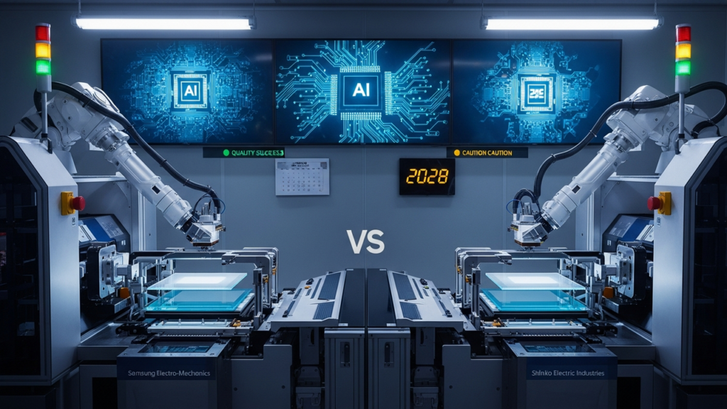
BusinessKorea South Korea Overview Samsung Electro-Mechanics (SEM) is accelerating its pursuit of glass substrates for AI chip packaging, targeting mass production by 2028 through its 'GlaSSEM' joint venture with Dongwoo Fine-Chem. This ... -
AI Accelerates Shift to Panel Level Packaging (PLP) and Glass Core Substrates, Positioning Them as Pillars of Next-Gen Packaging
IEEE / Presentation USA Overview Driven by soaring demand from AI, automotive electronics, and consumer devices, advanced packaging is a critical enabler for enhanced performance, higher integration, and miniaturization in semiconductors... -
ECTC 2026 Highlights Advanced Packaging Future: Glass Substrates and FOPLP at the Core of System Innovation
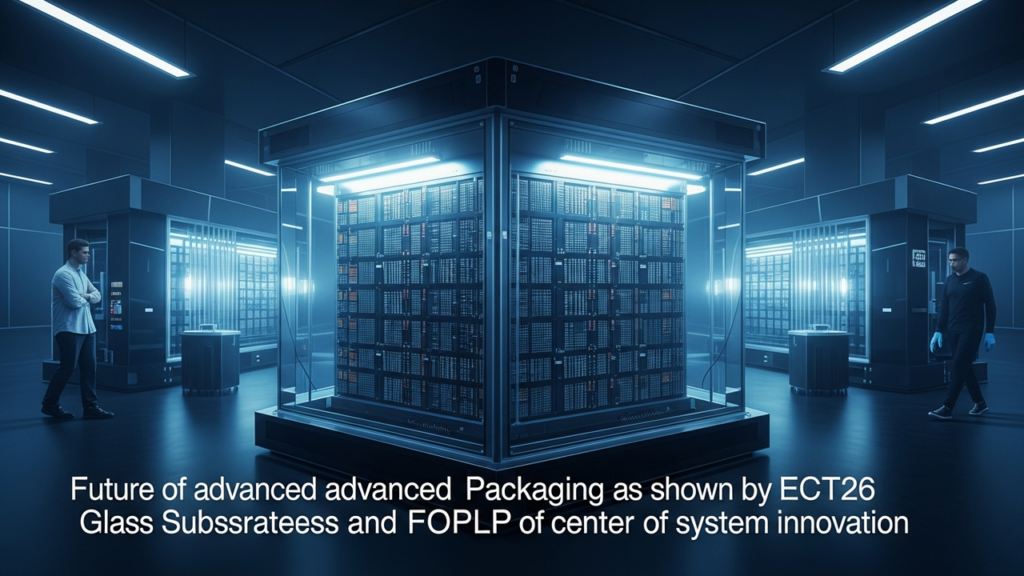
Advanced Packaging Magazine USA Overview ECTC 2026 emphasized a structural shift in semiconductor innovation, moving beyond transistor scaling to packaging and integration technologies. Noteworthy advancements in heterogeneous integratio... -
TrendForce Analyzes: 18 Chinese Enterprises Accelerate Positions in Glass Core Substrate Market
TrendForce Taiwan Overview TrendForce reported that 18 Chinese companies are rapidly enhancing their presence in the glass core substrate market for advanced packaging. This movement is part of China's strategy to achieve supply chain au... -
Glass Substrates Emerge as AI Packaging Game-Changer, Igniting Global Race Towards Mass Production as China and Japan Intensify Competition for Yield Stabilization
The Economy South Korea Overview As AI semiconductor competition shifts from process-node miniaturization to advanced packaging, China and Japan are intensifying efforts to lead the glass core substrate market, a cornerstone for next-gen... -
ASE Technology Bets Big on AI: $10.5 Billion Record Capex to Double Advanced Packaging by 2027
TrendForce Taiwan Overview ASE Technology Holding is significantly increasing its 2026 capital expenditure to a record $10.5 billion, aiming to double the revenue of its leading-edge advanced packaging (LEAP) business by 2027. This ambit...