Chiplet– tag –
-

Amkor Technology Commits $2.5B-$3.0B to Advanced Packaging Facilities for AI Demand, Arizona Plant Slated for 2028 Production
Hudson Labs USA Overview Amkor Technology plans a substantial capital expenditure of $2.5 billion to $3.0 billion for fiscal year 2026, driven by accelerating demand for advanced packaging in AI and data center computing. The investment ... -
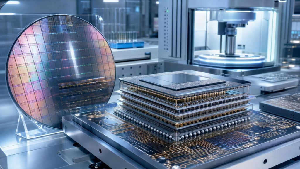
Lam Research Drives AI Performance with Advanced Packaging, Tackling Bottlenecks and Boosting Power Efficiency through Chiplets and Panel-Based Manufacturing
Lam Research USA Overview Lam Research highlights advanced packaging as the critical innovation frontier for AI, addressing the limitations of traditional semiconductor scaling. By enabling chiplets to function as a single system, this a... -
openPR.com Predicts AI Data Center Optical Interconnect Market to Reach $41.09 Billion by 2035, Driven by Intel’s Demonstrated Co-packaged Optics
openPR.com USA Overview This article provides an overview of a market research report published via openPR.com, forecasting the optical interconnect market in AI data centers to reach $41.09 billion by 2035. Growth is driven by increasin... -
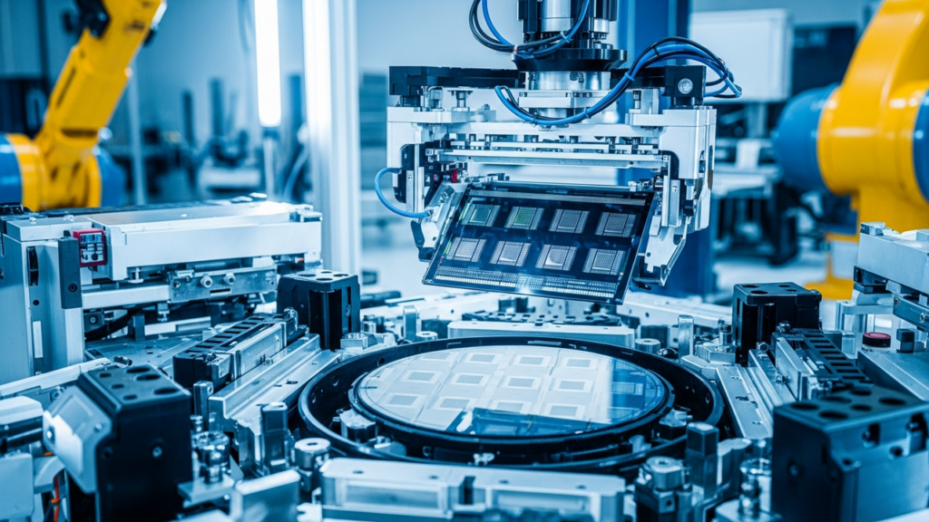
New Underfill Material Enables High-Performance Chiplet Integration in Fan-Out Wafer-Level Packaging
Semiconductor Packaging News Global Overview A new underfill material designed for Fan-Out Wafer-Level Packaging (FOWLP) has been developed, enabling next-generation high-performance chiplet integration. This material combines excellent ... -
Henkel Unveils High-Performance Underfill Material for Advanced Logic and Memory Packaging, Boosting Production Efficiency
Advanced Packaging Journal Germany Overview Henkel has introduced a new high-performance underfill material designed for advanced logic and memory packaging technologies like flip-chip and chiplets. This material significantly improves d... -
EU Chips Act Funds €210 Million for 3D IC Advanced Packaging, Benefiting Infineon, ASML Subsidiary, and Soitec
Qishuai-cn Germany Overview The European Commission announced its first EU Chips Act-funded project, allocating a total of €210 million to Germany's Infineon, an ASML subsidiary in the Netherlands, and France's Soitec. This funding is de... -
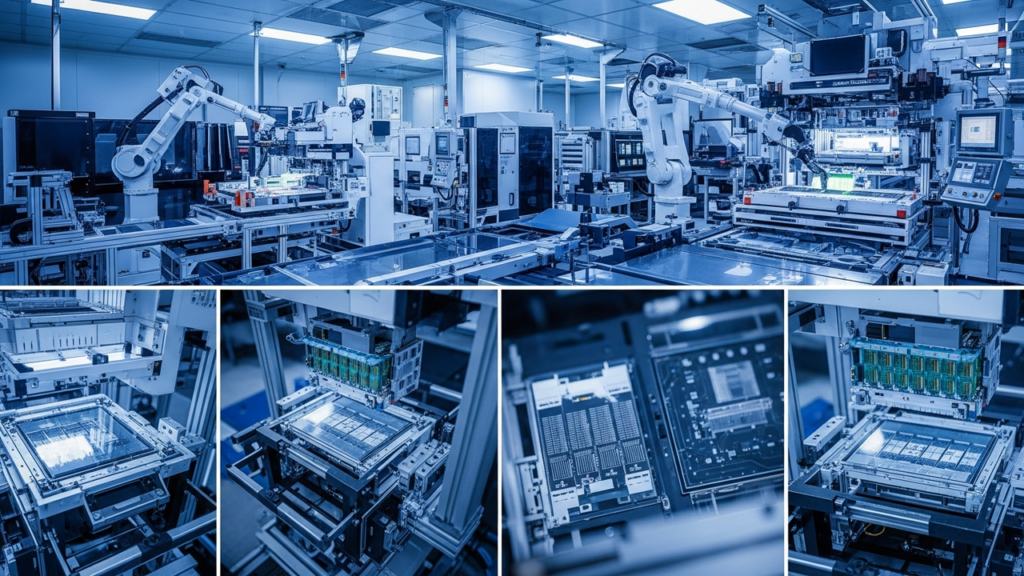
Applied Materials Unleashes Six New Systems to Turbocharge AI Chips with Advanced Packaging and Sub-10nm Defect Detection
Applied Materials USA Overview Applied Materials has launched six innovative systems to significantly accelerate the development and manufacturing of DRAM and advanced packaging for next-generation AI chips. These solutions tackle critic... -
Applied Materials Unveils New Systems to Propel DRAM & Advanced Packaging for AI Chips
StockTitan USA Overview Applied Materials has introduced a suite of new systems designed to dramatically enhance DRAM and advanced packaging processes, directly addressing the escalating performance demands of AI chips. These innovations... -
Ayar Labs Announces 50% Power Efficiency Boost and 3.2Tbps Bandwidth Expansion for Optical I/O Chiplets, Eliminating AI Accelerator Bottlenecks
Ayar Labs Blog USA Overview Ayar Labs has reported significant performance enhancements for its Optical I/O chiplets, achieving up to 50% improved power efficiency and extending chiplet-to-chiplet bandwidth to 3.2 terabits per second (Tb... -
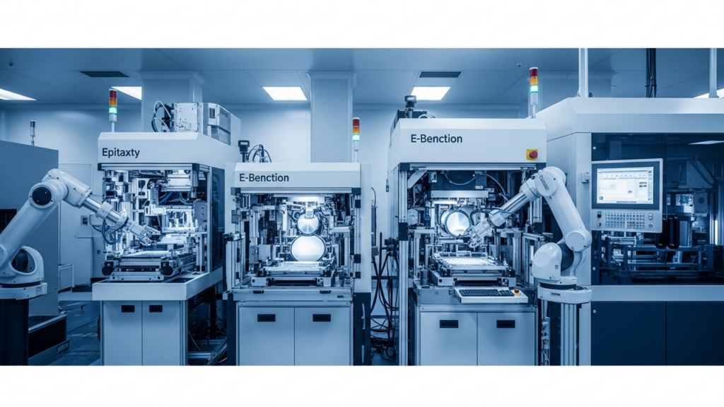
Applied Materials Unveils New Systems for DRAM and Advanced Packaging to Accelerate AI Chip Manufacturing, Featuring Epitaxy, CMP, and E-beam Inspection Technologies
Barchart.com USA Overview Applied Materials has introduced a suite of new chipmaking systems designed to accelerate the construction of advanced 3D chip architectures powering next-generation AI. This includes epitaxy systems optimizing ...