Chiplet– tag –
-

TSMC Accelerates CoPoS Packaging Development, Standardizing 310x310mm Panel Format; Introduces Glass Core Substrate for CoWoS Towards Late 2028 Mass Production
TrendForce Taiwan Overview TSMC is accelerating the development of its CoPoS (Chip-on-Panel-on-Substrate) packaging architecture, standardizing a 310x310mm panel format, with pilot production targeted for 2027 and mass production in late... -
Intel Appoints Former SK hynix CEO Lee Seok-hee as Senior VP of Advanced Packaging to Bolster AI Systems
The Korea Herald South Korea Overview Intel has appointed Lee Seok-hee, former CEO of SK hynix and SK On, as Senior Vice President of Intel Foundry. Lee will lead advanced packaging, system integration, back-end technology development, a... -
Lam Research Forecasts Over 50% Growth in Advanced Packaging Revenue by 2026, Emerging as a Key AI “Picks and Shovels” Provider
XTB.com USA Overview Lam Research, a leading semiconductor equipment manufacturer, predicts over 50% growth in its advanced packaging related revenue by 2026, driven by soaring demand for AI accelerators, HBM, and chiplet-based architect... -
imec Unleashes High-Density MIMCAP RF Interposer for D-Band Millimeter-Wave and Sub-THz Communications, Accelerating III-V Chiplet Integration
imec ベルギー Overview imec has unveiled a high-density MIMCAP RF interposer specifically engineered for demanding D-band and sub-THz wireless front-ends, alongside hundreds of gigahertz data center links. This innovative platform priori... -
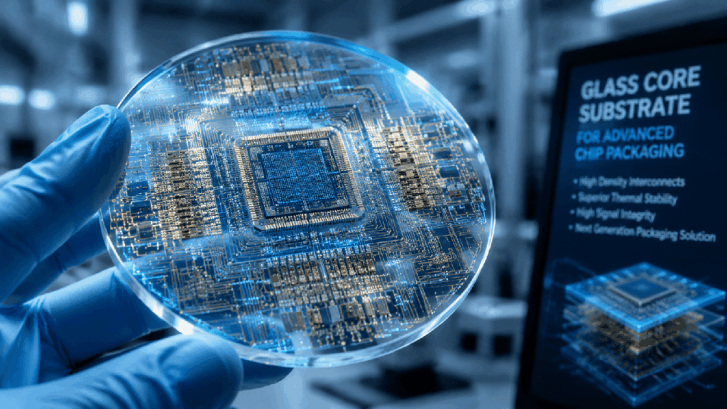
Glass Core Substrates Emerge as Next-Gen AI/HPC Packaging Technology, Face Commercialization Hurdles in Brittleness and TGV Formation
Pandaily China Overview Glass core substrates are garnering significant attention in the semiconductor packaging industry, driven by escalating performance demands in AI chips, HPC, and advanced processor packaging. They offer superior d... -
ABF Substrates Become AI Accelerator Bottleneck, Nvidia’s H100 Requires 12+ Layers; Glass Substrates Emerge as Next-Gen Solution, Commercialization Years Away
Data Gravity USA Overview Ajinomoto Build-up Film (ABF) substrates are a critical component and growing bottleneck in AI accelerators, HBM, and chiplet-based designs. Nvidia's H100 GPU demands over 12 layers of ABF, with the Blackwell B2... -
ECTC 2026: Intel Foundry and Amkor Announce Advanced Packaging Technologies for AI/HPC and U.S. Manufacturing Capacity Expansion
Intel Newsroom, Amkor Technology Blog, Semiconductor Engineering USA Overview The 2026 IEEE Electronic Components and Technology Conference (ECTC) showcased advanced packaging technologies redefining scalability limits for AI and high-pe... -
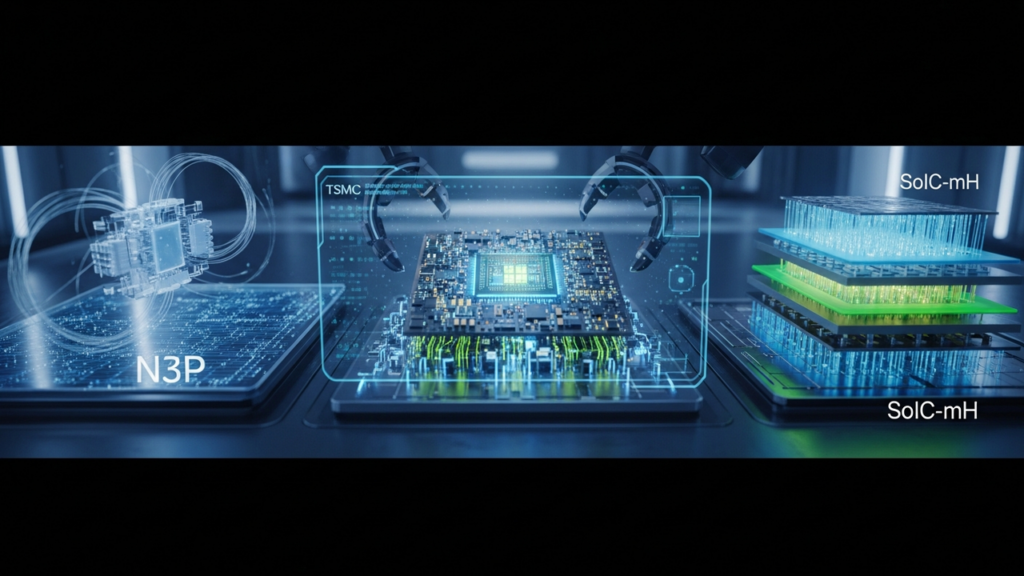
Apple’s M5 Ultra Pioneers Integration with TSMC’s N3P Process and SoIC-mH Packaging
TrendForce Taiwan Overview Reports indicate Apple's upcoming M5 Ultra chip, expected at WWDC, will likely leverage TSMC's N3P process node and its advanced SoIC-mH (System-on-Integrated-Chips – molded horizontal packaging) technology. So... -
Intel and Tesla Partner on AI6 Data Centers, Tapping Advanced Packaging for Production at Austin’s ‘Terafab’
Jamie's Substack USA Overview Tesla has announced a strategic partnership with Intel Foundry Services to scale its AI6 chip-powered data center clusters, extensively utilizing Intel's advanced packaging technologies. The collaboration wi... -
Advanced Packaging’s Evolution: 2.5D/3D Integration, Chiplets, and Hybrid Bonding Propel AI and HPC
Springer Professional Germany Overview Semiconductor packaging technology has dramatically evolved from 2D to 2.5D and 3D IC integration, a transformation accelerated by the explosive demand from AI and High-Performance Computing (HPC). ...