Chiplet– tag –
-

Hybrid Bonding Unlocks New Frontiers in 3D Integration, Driving AI Accelerators and Chiplet Designs
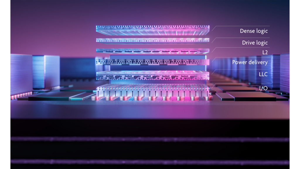
PatSnap UK Overview Hybrid bonding, an innovative 3D integration technology, enables both electrical continuity and mechanical integrity without solder or microbumps by combining metal-to-metal (primarily Cu-Cu) and dielectric-to-dielect... -
Intel Commits to Massive Advanced Packaging Push for Foundry Revival, EMIB Capacity Expansion Key
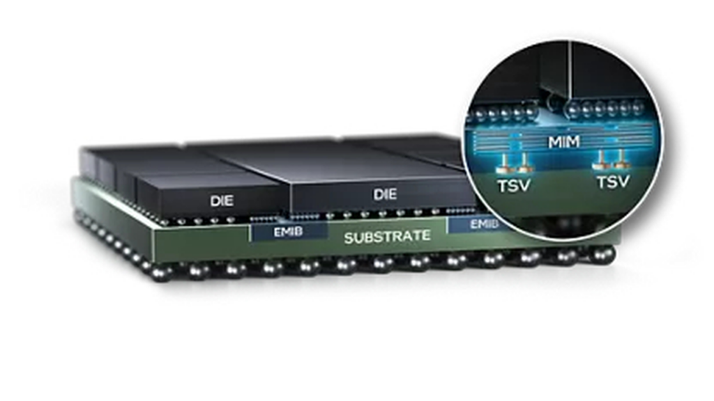
BusinessKorea USA Overview Intel is committing to a massive expansion of its advanced semiconductor packaging capabilities to accelerate its foundry business revival, with a core focus on expanding its proprietary EMIB (Embedded Multi-di... -
GlobalFoundries Triples Malta Fab Capacity with $16 Billion US CHIPS Act Investment, Targeting 1.5 Million Wafers/Year by late 2028
Tom's Hardware USA Overview GlobalFoundries is advancing a $16 billion US investment plan, bolstered by the CHIPS Act, to triple production capacity at its Malta fab. This includes an 11 billion Euro expansion at its Dresden plant, aimin... -
AMD Announces Over $10 Billion Taiwan Ecosystem Investment to Bolster AI Infrastructure and Advanced Packaging Manufacturing
Electronics Engineering Herald - EEHerald USA Overview AMD announced an investment exceeding $10 billion in Taiwan's ecosystem to expand its AI infrastructure and advanced packaging manufacturing capabilities. This significant capital in... -
CEA-Leti Demonstrates 1µm Pitch Die-to-Wafer Hybrid Bonding, Addressing AI Hardware Bottlenecks
Chiplet Marketplace France Overview CEA-Leti announced a significant advancement at ECTC 2026, demonstrating functional test vehicles utilizing die-to-wafer (D2W) hybrid bonding down to 1µm pitch, poised to resolve critical AI hardware b... -
Imec and EV Group Set New World Record for 3D Chip Stacking Precision with Sub-40nm Wafer Bond Overlay
PR Newswire ベルギー Overview Imec and EV Group have achieved a world-record post-bond overlay accuracy of less than 40 nanometers across a 300mm wafer for 200nm pitch hybrid bonding, a crucial advancement for next-generation 3D ICs. Dem... -
AMD Explores Powertech’s FOPLP for Next-Generation Zen 7 CPUs, Eyeing Packaging Diversification
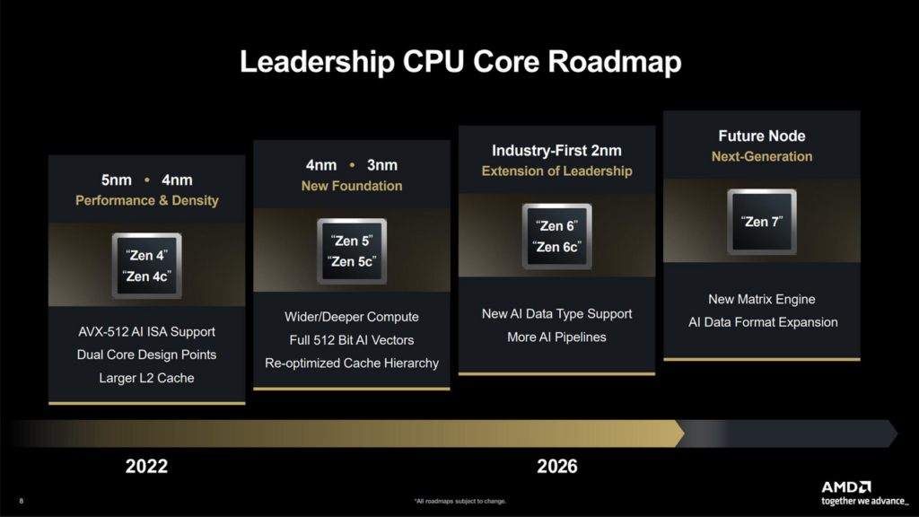
TechPowerUp USA Overview AMD is reportedly exploring Powertech Technology's Fan-Out Panel-Level Packaging (FOPLP) for its upcoming "Zen 7" CPUs, codenamed "Grimlock." This move signals AMD's strategic intent to build increasingly complex... -
ASE Unveils Industry-First Automated 310mm Panel-Level Packaging Line for AI and Chiplet Integration
AnySilicon Taiwan Overview Advanced Semiconductor Engineering (ASE) has developed an automated 310mm x 310mm panel-level packaging (PLP) production line, a significant advancement for AI processors and chiplet architectures. This industr... -
AMD Commits Over $10 Billion to Taiwan’s AI Ecosystem for Advanced Packaging and EFB Technology Expansion
EE Times Taiwan Overview AMD announced an investment exceeding $10 billion into Taiwan's AI ecosystem, bolstering advanced packaging capabilities and R&D. This initiative specifically targets Elevated Fanout Bridge (EFB) based 2.5D p... -
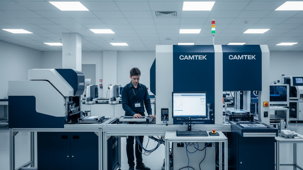
Camtek’s Precision Inspection and Metrology Solutions Drive Yield and Efficiency in Advanced Packaging
Camtek イスラエル Overview Camtek provides industry-leading 2D and 3D inspection and metrology platforms that address the escalating complexity and rapid growth of the advanced packaging market. Featuring sub-micron defect detection, CAD...