TROY TECHNICAL · BEGINNER’S GUIDE
READ THIS FIRSTNanotechnology — An Introduction
What changes when things get small? Connecting particles, films and surfaces.
Japanese version →Breaking a material into small particles or making it into a thin film can change its reactions and interaction with light. Nanotechnology is not simply a competition to make the smallest object. It uses structure at very small scales to obtain useful behaviour. Start with what size changes, rather than a catalogue of exotic material names.
01A nanometre is a unit of length
One nanometre is one billionth of a metre. This is much smaller than a hair, but “nano” does not name one substance. Particles, fibres, films and patterned surfaces can all have nanoscale dimensions. Their shapes and manufacturing methods differ.
The approximate range of 1–100 nanometres is a common introduction, not a universal product or legal definition. Ask which dimension is nanoscale. Particle diameter, film thickness and surface feature spacing describe different things.
Background: [1]
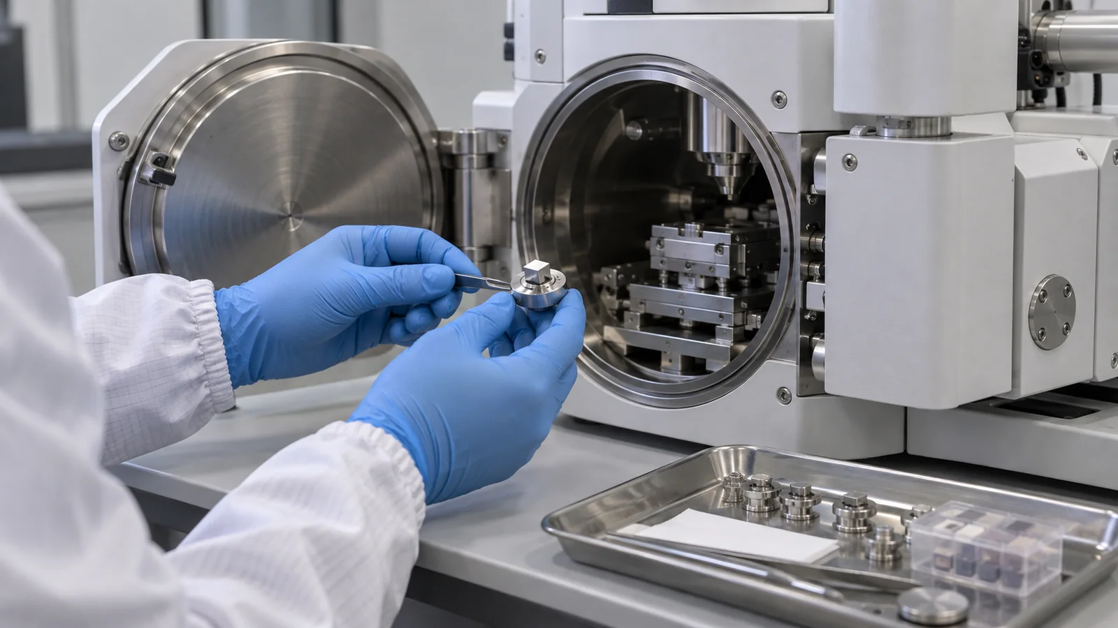
02Smaller pieces expose more surface
Dividing the same amount of material into smaller pieces increases its total exposed surface. That can provide more reaction sites in a catalyst and makes interfaces important in batteries and sensors. It can also increase unwanted reactions or degradation.
Small particles may aggregate. A good liquid dispersion can become larger clusters after drying. Adding a small amount of a remarkable material does not automatically transfer its properties to an entire product. Dispersion and surface treatment are part of the engineering.
Background: [1]
03Some structures also change electronic and optical behaviour
In semiconductor quantum dots, confinement of electronic states can change light absorption and emission. Composition and surface condition also matter, so colour alone does not uniquely determine size. Not all nanomaterials glow.
Other techniques build very thin layers or pattern small features to guide light or control electrical pathways. Working with dispersed particles and fabricating a structured surface are different routes within the same broad field.
Background: [1]
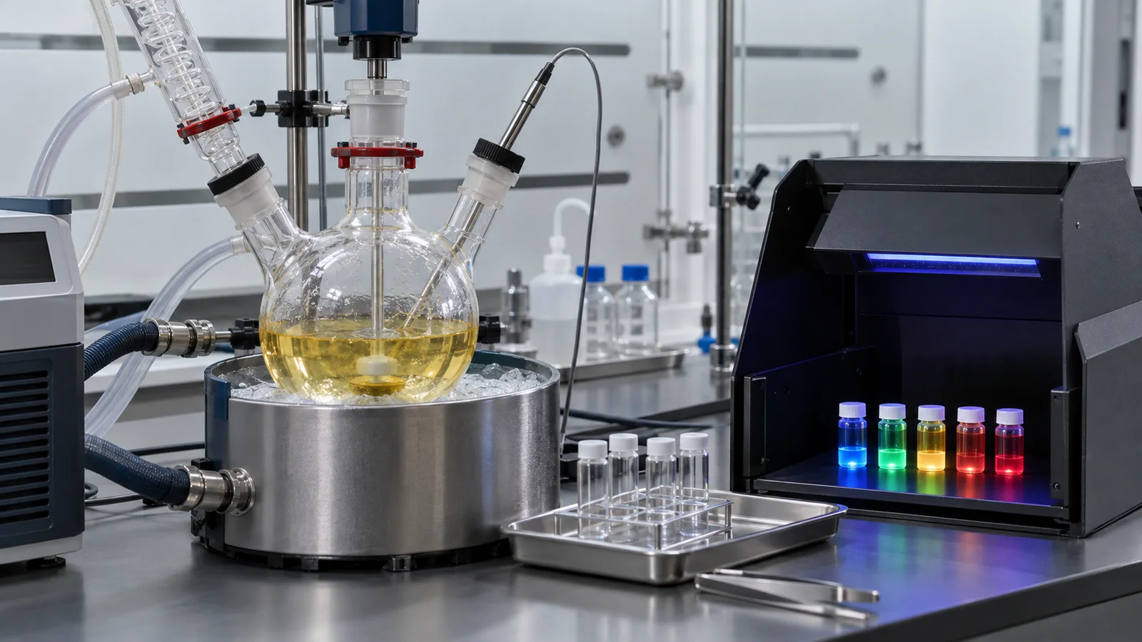
04Pair fabrication with measurement
Structures can be made by removing material from a larger object or by assembling smaller building blocks. Lithography transfers patterns; etching removes selected material; atomic layer deposition, or ALD, grows films through repeated surface reactions. Ask what is being placed or removed, where, and in what amount.
A dimension measured in a microscope and a size inferred from motion in a liquid need not describe the same thing. An average alone hides variation and aggregation. Check the measurement principle, sample preparation and whether a distribution is weighted by number or volume.
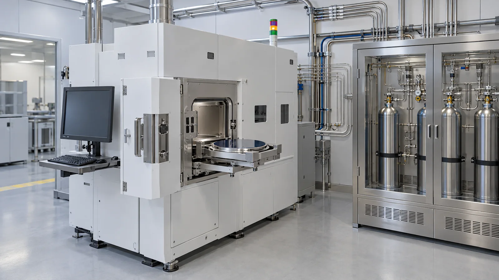
05Judge usefulness and safety by the actual material and use
Evaluation depends on composition, shape, size, surface treatment, released quantity and exposure routes such as inhalation or skin contact. Neither “nano means dangerous” nor “natural means safe” is a sufficient conclusion.
Particles fixed in a polymer and airborne powder can expose people very differently even if their composition is identical. Manufacturing, wear and recovery matter alongside use. The reading routes separate materials, fabrication, measurement and applications so that these questions stay connected.
Background: [2]
Connect the ideas in one situation
ILLUSTRATIVE SCENARIO — NOT A PERFORMANCE CLAIM
Suppose particles are added to a transparent polymer
A useful particle function may come at the expense of transparency if clusters scatter light. Examine aggregation, concentration, surface treatment and compatibility with the polymer, not just primary particle size.
Test the desired function and transparency in the finished material. What matters is whether the needed structure survives processing. This connects material design, dispersion, manufacturing and measurement.
Return to the starting idea
Nanoscale behaviour depends on shape, surfaces and surroundings as well as size. The goal is to make and verify the right structure, not assume that smaller is always better.
You do not need to memorize every technology name. Understanding the intended improvement, the mechanism being changed and the conditions needed to demonstrate it gives you a foundation for the detailed articles. Choose one route that matches your question.
Choose your next article
Read a route from top to bottom, or select just the question you need. You do not have to read everything.
Begin with measurement
Make structures and surfaces
Choose an application
Browse all technical articles in this field (28)
- Drug Delivery Systems and Targeting
- MXenes and Nanosheets
- mRNA Medicines and Lipid Nanoparticles
- Etching
- Carbon Nanotubes
- Graphene
- Silicon Anodes and Nanostructured Electrodes
- Supercapacitors
- Theranostics and Nano Contrast Agents
- Nanocoatings and Thin Films
- Nanoscale Transistors
- Nanofibers and Electrospinning
- Nanoscale Memory
- Nanomaterial Definitions and Regulation
- Nanoparticles and Nanozymes
- Nanometrology
- Plasmonics and Nanophotonics
- Perovskite Basics
- Polymer Blends and Fillers
- Lithography and EUV
- Liposomes and Nanocarriers
- Resists and Photomasks
- Titanium Dioxide and Photocatalysis
- Atomic Layer Deposition (ALD)
- Lipid Nanoparticles
- Self-Assembly and Nanoimprint
- Quantum Dots
- Metal-Organic Frameworks (MOFs)
Sources and scope
This introductory synthesis connects the existing technical articles. Its grouping and design scenarios are explanatory, not standard classifications or test results. It does not catalogue current records, product availability or approvals, or forecast costs. Foundational references are below; linked articles provide more detailed technical sourcing.